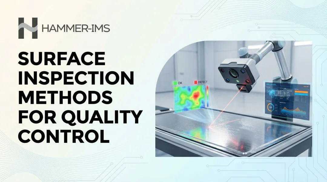
Introduction
A single undetected particle measuring just 20 nanometers on a wafer surface can render an entire chip unusable. At advanced 3nm nodes, wafer processing costs reach €18,500 to €23,000 per wafer. That makes surface inspection far more than a quality checkpoint — it's an economic imperative.
As device geometries shrink and structural complexity increases — especially with 3D architectures and high-aspect-ratio features — inspection requirements have intensified. Manufacturers now deploy a range of surface inspection methods, from optical and laser-based scanning to electron beam and atomic force probe techniques, each with distinct trade-offs between resolution, throughput, and detection depth.
Given what's at stake per wafer, choosing the right inspection approach matters. This article covers the main methods, how they fit into manufacturing workflows, and how to match each technique to your quality control requirements.
Key Takeaways
- Wafer surface inspection detects particles, scratches, pits, microcracks, and pattern anomalies that cause yield loss
- Multiple methods exist: optical (brightfield/darkfield), laser scanning, SEM, AFM, infrared, and e-beam inspection
- Each method balances resolution, speed, and defect type—most fabs use combinations rather than single techniques
- AI-powered automated defect classification reduces false positives by 38–46%, integrating directly with statistical process control systems
- Method selection hinges on wafer type, defect scale, production volume, and whether inspection runs inline or offline
What Is Wafer Surface Inspection?
Wafer surface inspection is the systematic process of examining semiconductor and substrate wafer surfaces to detect physical and pattern defects—particles, scratches, voids, crystal defects, and dimensional deviations—at various stages of the fabrication workflow. Catching these anomalies early prevents them from propagating through costly downstream processing steps.
Two Primary Inspection Categories
Patterned wafer inspection uses die-to-die or die-to-database comparison to detect random and systematic defects. By comparing the image of a test die with an adjacent die, the system highlights anomalies that don't cancel out in the subtraction process, creating a defect map that pinpoints irregularities across repeated circuit patterns.
Non-patterned (bare) wafer inspection detects surface anomalies directly via light scattering or probe methods—no image comparison needed. Without a reference pattern, these systems detect changes in reflected or scattered light to identify particles, scratches, and crystal defects on unprocessed silicon.
Where Inspection Fits in the Fabrication Workflow
Inspection is typically performed at three critical stages:
- After wafer creation – Detecting crystal growth anomalies and polishing residues
- During incoming quality control – Verifying supplier wafer quality before fab processing
- During/after microchip development – Monitoring process-induced defects throughout fabrication
Each stage demands a different tradeoff: post-creation checks prioritize sensitivity to subtle surface defects, while in-line fabrication monitoring must also maintain the throughput needed to keep production moving.
Why Wafer Surface Inspection Is Critical for Quality Control
The financial stakes are clear: a single semiconductor manufacturer lost nearly €63 million across eight major production steps due to yield losses. Any undetected flaw that propagates through subsequent process steps multiplies in cost, making early-stage inspection far more economical than late-stage scrap or rework.
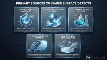
Primary Sources of Wafer Surface Defects
Understanding where defects originate helps explain why inspection must be continuous rather than a final checkpoint:
- Crystal growth anomalies – Crystal-originated particles (COPs) and structural voids formed during ingot growth
- Slicing and polishing residues – Mechanical damage from wire sawing and CMP processes
- Cleaning process failures – Particle contamination from incomplete chemical or ultrasonic cleaning
- Handling-induced scratches – Mechanical damage during wafer transport and handling
- Environmental contamination – Airborne particles deposited during fabrication
Operational Benefits of Robust Inspection Programs
Effective inspection delivers measurable advantages:
- Catches defects early, preventing costly rework on partially processed wafers
- Enables real-time process adjustments before variations affect entire batches
- Integrates with statistical process control (SPC) so teams can intervene before batch-wide failures occur
- Identifies repeating defect patterns from mask or exposure conditions before they spread across all dies on a wafer
Key Surface Inspection Methods Explained
No single inspection method dominates because each offers distinct strengths in resolution, throughput, and defect type sensitivity. Modern fabs use combinations tailored to specific process stages and quality requirements.
Optical Inspection (Brightfield and Darkfield)
Optical inspection illuminates the wafer surface with visible or ultraviolet light and detects anomalies via changes in contrast, reflection, or light scattering.
Brightfield mode identifies surface features through intensity changes—lights are oriented between 90° and 45° from the imaging surface, targeting high-sensitivity applications but delivering lower inspection throughput.
Darkfield mode captures scattered light to highlight particles and edge defects with higher contrast. Lights are oriented between 0° and 45° off horizontal, making this mode particularly effective for imaging highly reflective surfaces and detecting particles or scratches on bare wafers.
Key advantages:
- Fast, non-contact operation compatible with automated inline systems
- High throughput—up to 100 wafers per hour for 300mm wafers at 10µm pixel resolution
- Optical far-field inspection takes about 88% of the wafer inspection market
Limitations:
- Lower resolution than electron-based methods
- Limited sensitivity to subsurface flaws
- Diffraction-limited resolution (~200 nm for visible light)
Laser Scanning Inspection
A focused laser beam is rastered across the wafer surface and photodetectors capture reflected or scattered light to map surface topography and identify particles, pits, or protrusions. Laser scanning operates in two modes:
- Topographic mode – Detects height variations and surface roughness
- Scattering mode – Identifies contamination and particles
Performance characteristics:
- Detects particles as small as 20 nm
- Well-suited for high-throughput production environments
- Requires calibration for different surface materials
Systems like the KLA Puma 9980/9850 provide high-throughput production ramp monitoring for advanced patterning layers, making them well-established tools for inline critical defect monitoring at volume scale.
Electron Beam and Scanning Electron Microscopy (SEM)
E-beam and SEM systems direct a focused electron beam at the wafer surface and detect emitted secondary or backscattered electrons to produce high-resolution images at the nanometer scale. E-beam inspection also detects voltage contrast differences to identify conductivity issues in high-aspect-ratio structures—electrical opens and shorts that optical methods cannot detect.
Traditional single-beam e-beam inspection locates defects down to 1 nm, but its ultra-small field of view severely limits throughput—making it unsuitable for inline high-volume manufacturing. Conventional SEM is typically reserved for defect review and R&D.
Multibeam tools are changing that. The ASML HMI eScan 1100 features 25 electron beams, increasing throughput by up to 15 times compared to single e-beam tools while detecting patterning defects down to 7 nm—shifting e-beam from an offline review tool into a viable inline monitoring option.
Atomic Force Microscopy (AFM)
AFM operates by scanning a sharp probe systematically over the surface with a piezoelectric scanner, while cantilever deflections tracked by a laser and photodetector create a 3D topographic map with sub-nanometer resolution. It measures surface roughness, nanoscale scratches, and crystal defects with sub-angstrom vertical precision.
Systems like the Bruker InSight 300 demonstrate what this precision looks like in practice: noise floors below 35 picometers and scanner flatness of ±1nm.
Practical limitations:
- Scan area is narrow — typical measurements cover one site per minute, or several minutes for 100 µm scans
- Throughput is too low for whole-wafer inline inspection
- Best suited to R&D, process development, and failure analysis where precision outweighs speed
Subsurface Methods: Infrared (IR) and X-Ray Inspection
While most surface inspection focuses on visible defects, subsurface integrity matters for unpatterned wafers and advanced packaging applications.
Infrared inspection exploits silicon's transparency to infrared light to detect internal cracks, voids, and dislocations. Using a 1310 nm laser or broadband halogen source, IR microscopy locates defects—particles, CMP damage, voids—at the interface of bonded wafer pairs, with overlay measurement repeatability of less than 0.1 µm. This makes IR inspection particularly valuable for detecting bonded interface defects invisible to surface optical tools.
X-ray inspection uses high-energy radiation to image internal structures, particularly for advanced packaging, 3D ICs, and through-silicon vias (TSVs). X-ray techniques reveal voids within copper-filled TSVs and solder bumps, providing submicron 3D imaging for non-destructive failure analysis of complex 2.5D/3D architectures.
Trade-offs: Both methods are non-destructive but offer lower surface resolution than optical or electron-based approaches. In practice, they are most effective when layered into inspection workflows alongside optical or e-beam tools at specific process checkpoints.
AI-Augmented Automated Defect Classification (ADC)
ADC systems automatically assign detected defect signals to specific categories, enabling engineers to build a classified defect Pareto that identifies yield-limiting defect types and supports faster root cause analysis.
In advanced 3D architectures like Gate-All-Around (GAA) structures, optical inspection false alarm rates can exceed 90%—and traditional rule-based classifiers struggle to keep up. Modern ADC tools address this with deep learning models that classify both known and novel defect types across diverse wafer designs. Applied Materials combines cold field emission imaging with deep learning AI to automatically extract true defects from nuisance defects with nearly 100% accuracy, handling 10,000 candidates in less than an hour.
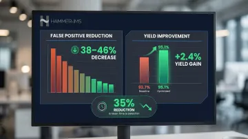
Integrated process control: AI-driven ADC systems reduce false positives by 38–46% and improve average process yield from 92.7% to 95.1% while cutting mean time to detection by 35%. Integrating ADC with SPC systems enables predictive process control rather than purely reactive quality management.
How Surface Inspection Integrates into the Wafer Manufacturing Workflow
Wafer inspection runs as a continuous quality loop across multiple process stages: post-growth bare wafer qualification, incoming inspection at the fab, in-process monitoring after critical deposition or etch steps, and final outgoing inspection before packaging. Each stage targets a different failure mode, which is why no single tool or checkpoint is sufficient on its own.
Inline vs. Offline Inspection
Inline systems integrate directly into the production line for real-time feedback and minimal latency. These tools prioritize throughput and non-contact operation, enabling 100% sampling without production bottlenecks. Optical and laser scanning systems dominate inline inspection due to their speed and automation compatibility.
Offline systems like SEM and AFM provide deeper analysis but are used selectively on flagged wafers to avoid throughput bottlenecks. These tools offer higher resolution and more detailed characterization but cannot inspect every wafer without creating production delays.
Statistical Process Control (SPC) Integration
Defect data from inspection systems feeds into SPC frameworks, enabling engineers to:
- Identify process drift before it reaches yield-impacting levels
- Isolate systematic defect signatures tied to specific equipment or process steps
- Implement closed-loop corrections to deposition, etch, or cleaning parameters
- Shift from reactive firefighting to predictive process optimization
Defect Maps and Coordinate Data
Inspection systems record the X/Y position coordinates of all detected anomalies, creating defect maps that allow engineers to distinguish between random and systematic failure modes.
| Defect Type | Typical Cause | Corrective Action |
|---|---|---|
| Random | Particles or environmental contamination | Contamination control, handling protocol changes |
| Systematic | Mask defects, exposure errors, equipment misalignment | Equipment calibration, mask corrections |
Coordinate-level classification is what makes root cause analysis tractable — without positional data, distinguishing a contamination event from a recurring equipment fault is largely guesswork.
How to Choose the Right Inspection Method
| Inspection Method | Spatial Resolution | Throughput | Best-Suited Defect Type | Inline/Offline |
|---|---|---|---|---|
| Optical (Brightfield/Darkfield) | ~200 nm (visible); SR-DUV extends limits | High (up to 100 WPH) | Particles, scratches, pattern defects | Inline HVM |
| Laser Scanning | High sensitivity for patterning layers | High | Critical defects, systematic nuisance | Inline HVM |
| SEM / E-Beam (Single) | Down to 1 nm | Low | Physical defects, voltage contrast | Offline review |
| E-Beam (Multibeam) | Down to 7 nm | Medium (15x faster than single) | Patterning defects, voltage contrast | Inline excursion monitoring |
| AFM | <35 pm vertical | Very Low (~1 min per site) | 3D topography, sidewall roughness | Offline/targeted inline |
| Infrared (IR) | ~0.5 µm | Medium | Bonded interface voids, particles | Inline bonded pairs |
| X-Ray / CT | Submicron (<1 µm) | Low to Medium | TSV voids, solder bump cracks | Offline FA |
Two Key Selection Criteria
Wafer type:
- Patterned wafers require die-comparison-based systems (optical or e-beam with pattern recognition)
- Non-patterned wafers are better served by laser scanning or optical scattering methods that detect anomalies directly
Production context:
- High-volume fabs prioritize throughput and inline capability—optical and laser scanning dominate
- R&D or process development environments prioritize resolution and characterization depth—SEM and AFM provide detailed analysis
Complementary Measurement for Dimensional Uniformity
For dimensional uniformity and thickness-related parameters—particularly in substrate and advanced materials manufacturing—non-contact measurement systems add value alongside optical defect inspection. Hammer-IMS's M-Ray technology uses millimeter wave measurement to deliver continuous, real-time thickness and surface uniformity monitoring across industrial materials, enabling process corrections before variations become yield-impacting defects.
How Hammer-IMS Supports Quality and Process Control in Advanced Manufacturing
Hammer-IMS provides non-contact, non-nuclear measurement systems using M-Ray (millimeter wave) technology, enabling continuous, real-time thickness and surface uniformity monitoring across industrial materials including wafers and substrates. This contactless approach avoids surface contamination risks, supports clean manufacturing environments, and provides closed-loop process feedback to prevent defects from forming rather than just detecting them after the fact.
Key differentiators for quality-conscious manufacturers:
- Real-time data logging – Every measurement is captured continuously, giving operators the data they need to catch process drift before it causes defects
- Remote connectivity – Connectivity 3.0 software supports remote monitoring and diagnostics without requiring on-site intervention
- Closed-loop production adjustment – Measurement feedback automatically corrects process parameters, keeping thickness tolerances tight across the full production run
- Non-nuclear, non-contact operation – No radioactive sources means no regulatory licensing overhead and no risk of surface contamination from the sensor itself
Together, these capabilities move quality management upstream. Instead of catching defects at end-of-line inspection, manufacturers can correct process conditions in real time and reduce material waste across the run.
Frequently Asked Questions
What are the most common types of defects found on wafer surfaces?
The most common defects include particles (dust, residue), scratches from mechanical handling, crystal defects such as COPs (crystal-originated particles), pits, microcracks, and pattern defects caused by lithography or etch process variations.
What is the difference between patterned and non-patterned wafer inspection?
Patterned wafer inspection uses die-to-die or die-to-database image comparison to detect defects amid circuit structures. Non-patterned (bare) wafer inspection detects anomalies directly via laser scattering or other methods since there's no reference pattern to compare against.
Which wafer surface inspection method offers the highest resolution?
AFM and SEM offer the highest spatial resolution—AFM achieves sub-nanometer vertical precision (below 35 picometers) while SEM reaches nanometer-scale lateral resolution down to 1 nm. Both have throughput limitations that make them better suited to defect review and R&D rather than high-volume inline inspection.
How does automated defect classification improve wafer quality control?
ADC automatically categorises detected defects by type, enabling faster root cause analysis, yield excursion monitoring, and SPC integration for predictive process control. AI-driven ADC reduces false positives by 38–46% and improves average process yield from 92.7% to 95.1%.
What is the role of non-contact measurement in wafer surface inspection?
Non-contact measurement technologies, such as optical, laser, and millimeter wave systems, inspect wafer surfaces without touching them. This prevents contamination and mechanical damage while enabling continuous inline monitoring at production speeds — ideal for clean manufacturing environments and high-throughput lines.
How often should wafer surface inspection be performed during manufacturing?
Inspection typically occurs at three stages: after wafer creation, during incoming QC at the chip fab, and during/after microchip development. Additional inline monitoring follows critical process steps — deposition, etch, and CMP — to catch process-induced defects early.