
This guide explains what wafer inspection is, the primary optical, electron beam, and measurement techniques used, where inspection gates are placed in the manufacturing flow, and how inspection data drives continuous process improvement and yield recovery.
TLDR:
- Wafer inspection detects surface defects, pattern errors, and dimensional irregularities before costly processing accumulates
- Fabs combine optical, e-beam, and dimensional measurement to balance throughput and nanometer-scale sensitivity
- Inline inspection at critical gates—post-lithography, post-etch, post-CMP—prevents defective wafers from advancing
- Spatial defect mapping and AI-driven data analysis turn raw inspection results into automated process corrections and predictive maintenance triggers
What Is Wafer Inspection?
Wafer inspection is the systematic examination of semiconductor wafers to detect physical defects, pattern anomalies, and dimensional irregularities. It covers both surface-level issues—particles, micro-scratches, and incomplete etch patterns—and subsurface concerns, including voids, thickness variation, and wafer bow or warp. Inspection tools use optical imaging, electron beams, or contactless measurement to identify defects at different stages of the manufacturing flow.
The two primary wafer states under inspection call for distinct approaches. Patterned wafers carry circuit features—transistors, interconnects, vias—built layer by layer through lithography and etch. Inspection systems compare die-to-die or die-to-database to detect pattern defects, overlay errors, and missing features.
Non-patterned (bare) wafers, by contrast, are unpatterned silicon substrates checked before fabrication begins. Laser scattering methods identify particles, crystal defects, and surface scratches that could compromise every subsequent process step.
Wafer inspection goes well beyond spotting problems. Each defect is classified by type—particle, residue, or scratch—and logged with exact X-Y position coordinates. Those results get correlated to specific process steps or tools, then fed back into yield engineering workflows.
This data-driven feedback loop allows fabs to isolate root causes, trigger automated lot holds, and adjust process recipes before excursions escalate.
That sensitivity to substrate conditions explains why incoming wafer quality matters so much. Silicon wafers are the physical foundation on which integrated circuits are built—flatness, purity, and dimensional consistency affect every lithography, deposition, and etch step that follows. A wafer with excessive bow or thickness variation will lose focus during lithography, producing defective patterns before any contamination even enters the picture.
Why Wafer Inspection Matters: Yield, Cost, and Reliability
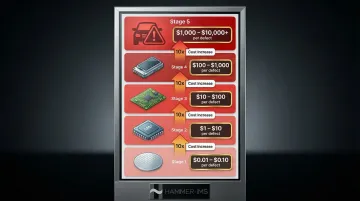
At advanced nodes, even a single killer defect on a die can render it unusable. When a flawed wafer continues through 20+ additional process steps before being caught, the accumulated cost per wafer becomes significant. Manufacturing a 3nm wafer costs $19,500, reflecting the extreme complexity of EUV lithography and multi-patterning. Early yield rates at this node hover around 50–60%, meaning nearly half of the chips on a wafer may be defective.
Inline inspection allows fabs to identify and remove defective wafers early, preventing unnecessary processing, rework, and material waste. This cost-control benefit is quantified through a Cost of Non-Quality (CONQ) baseline that merges finance and engineering data to measure the true monetary impact of yield losses, justifying heavy investments in inspection capital.
Cost, however, is only part of the picture. Industries such as automotive, aerospace, and medical electronics demand near-zero defect rates in finished chips. Automotive applications governed by AEC-Q100 and IATF 16949 standards are pushing quality targets from 10 defective parts-per-million (Dppm) to 10 defective parts-per-billion (Dppb).
Latent defects are particularly difficult to manage. These include:
- Partial metal lines that pass continuity tests but fracture under thermal cycling
- Gate oxide pinholes that survive initial burn-in but degrade over time
- Contact residues that cause intermittent failures months into field operation
The cost of discovering a defect increases 10x at every subsequent supply chain level. A defect caught on the wafer costs cents to address; the same defect found in a recalled vehicle can cost thousands.
Types of Wafer Inspection Techniques
Optical Inspection — Brightfield and Darkfield
Brightfield inspection detects reflectance changes caused by pattern defects, missing features, and overlay shifts. It collects reflected light with illumination oriented perpendicular to the wafer, providing a realistic view of patterned features. Brightfield is effective for patterned wafer comparison, using die-to-die or die-to-database subtraction to isolate defects.
Darkfield inspection captures scattered light rather than reflected light, making it highly sensitive to surface particles, micro-scratches, and edge defects that generate minimal reflected contrast. Illumination is oriented at a shallow angle, and the system collects light scattered by surface irregularities. Deep Ultraviolet (DUV) 193nm lasers extend darkfield sensitivity to sub-pitch features at advanced nodes, enabling systems like the Applied Materials DFinder to detect particles down to 40nm on patterned wafers.
Optical inspection struggles with sub-20nm defects due to diffraction limits and pattern noise from complex 3D structures, requiring fabs to supplement optical tools with higher-resolution methods.
Electron Beam (E-Beam) Inspection
E-beam systems irradiate the wafer surface with electrons and detect secondary electrons (SE) for surface topography and backscattered electrons (BSE) for deep or buried structures. This approach achieves nanometer-scale resolution—typically 1 to 3 nm—capable of imaging deep pattern details and detecting ultra-thin residues at contact hole bottoms.
E-beam is uniquely suited for Voltage Contrast (VC) inspection. By measuring the build-up of surface potential, VC inspection detects buried electrical defects such as contact hole residues, thin nitride remains, and electrical opens or shorts that optical tools cannot see.
The trade-off is throughput. E-beam is significantly slower than optical systems, limiting its use to hotspot review and R&D applications. To address this, OEMs are developing multi-beam systems like the ASML HMI eScan 1000, which uses a 3x3 array of nine electron beams, increasing throughput by up to 600% over previous single-beam tools.
Non-Patterned (Bare) Wafer Inspection
Bare wafer inspection uses laser scattering to detect particles, pits, and crystal defects on unpatterned surfaces. A laser beam is projected onto the rotating wafer and moved radially to cover the entire surface in a spiral or radial scan pattern.
Particles or defects scatter that light, captured by multiple detection channels—darkfield, phase contrast, and photoluminescence. Each channel records both position coordinates and defect type, distinguishing particles from crystal defects such as COPs.
Modern production tools like the KLA Surfscan SP7 achieve an industry-leading defect sensitivity of 12.5nm, critical for R&D pathfinding at ≤5nm logic nodes. This method is used at wafer incoming inspection, equipment cleanliness monitoring, and bare wafer qualification.
Non-Contact Dimensional and Thickness Measurement
Beyond surface defects, wafer inspection encompasses physical attribute verification—including thickness uniformity, flatness, bow, and warp—which directly affect lithography focus, CMP uniformity, and downstream process control. High Total Thickness Variation (TTV) consumes the lithography depth-of-focus budget and degrades CMP performance, leading to dishing and erosion.
SEMI M1 standards define nominal thicknesses: 625 µm for 150mm wafers, 725 µm for 200mm wafers, and 775 µm for 300mm wafers. Fabs measure TTV, flatness, bow, and warp using contactless methods like capacitance gauges and coherence scanning interferometry.
Contactless, non-nuclear measurement technologies—such as Hammer-IMS's M-Ray millimeter wave systems—offer a clean, radiation-free method for measuring thickness uniformity without physical contact, preserving wafer integrity during incoming qualification.
These systems operate using electromagnetic millimeter waves at 60 GHz, transmitting a signal through the material that reflects off the bottom surface and returns to the sensor for analysis. The result: precise thickness measurement with no radioactive sources and no special licensing requirements.
Specialized and Emerging Techniques
Additional methods address niche defect classes and 3D architectures:
- Infrared (IR) imaging: Silicon is transparent to IR radiation. Systems use Short Wavelength Infrared (SWIR) to measure overlay and detect internal voids or cracks in bonded wafer pairs for 3D heterogeneous integration
- X-ray inspection: Non-destructive 3D imaging of Through-Silicon Vias (TSVs) and advanced packaging structures. Systems like the ZEISS Xradia Context achieve spatial resolutions of 0.95 µm
- Atomic Force Microscopy (AFM): Provides atomic-scale 3D topography with <30 pm RMS Z-noise floor and ~0.1 nm vertical resolution, essential for R&D and failure analysis
- 3D metrology: Advanced 3D optical critical dimension (OCD) scatterometry measures tungsten recess in high-aspect-ratio (HAR) 3D NAND slits (96+ layers) to prevent wordline shorts
Why Fabs Combine Multiple Techniques
No single inspection technology covers all defect classes. Optical tools offer high throughput but taper off at sub-10nm sensitivity due to the Rayleigh scattering limit. E-beam catches the finest defects—down to 1 nm—but cannot scan full wafers at production speed. Dimensional measurement tools verify substrate geometry but do not detect particles or pattern defects.
| Feature | Optical Brightfield | E-Beam Inspection |
|---|---|---|
| Defect Sensitivity | ~20–30 nm | 1–3 nm |
| Throughput | High | Low |
| Primary Use Case | Full wafer, fab control | Hotspot, R&D, review |
| Inspection Type | Surface & pattern | Physical, electrical, buried |
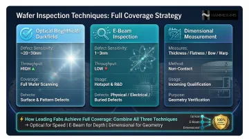
Fabs combine methods strategically: optical systems quickly scan full wafers and flag hotspots, which are then reviewed by high-resolution e-beam tools. This multi-modal strategy maximizes defect coverage without sacrificing cycle time.
Key Stages of Wafer Inspection in the Manufacturing Flow
Incoming Bare Wafer Inspection
Before any processing begins, wafers are checked for particles, scratches, crystal defects, edge chips, and dimensional attributes (thickness, flatness, warp). This is the last opportunity to reject bad substrates before costly fabrication value is added.
Front-End-of-Line (FEOL) and Post-Lithography/Post-Etch Inspection
Inspection gates are placed after high-risk steps such as oxidation, implant, and each lithography-etch cycle to catch surface contamination, overlay errors, line-edge variation, and stochastic defects early. Post-lithography (After-Develop Inspection, or ADI) ranks as one of the most critical checkpoints in the entire flow. Inspecting the photoresist allows the wafer to be reworked (stripped and reprinted) if defects are found, saving the wafer from being scrapped.
Post-etch inspection detects incomplete etches, microbridges, and line breaks, as etch steps can enlarge latent lithography pinholes, making them visible.
CMP, BEOL, and Pre-Passivation Inspection
Each stage in this phase targets a distinct category of defects:
- CMP: Scratches, dishing, and slurry residue following chemical mechanical planarization
- BEOL layers: Voids, shorts, and cracks in metal and dielectric structures
- Pre-passivation: Final pattern verification to confirm structural integrity before electrical probe testing
The Wafer Inspection Workflow: From Loading to Data Feedback
Wafer Loading, Recipe Setup, and Alignment
Automated handlers transfer wafers from the FOUP to the inspection tool without introducing contamination, governed by SEMI standards E84 and E87 for SECS/GEM communication. The tool reads the wafer ID and aligns to the notch or flat. It then selects the appropriate inspection recipe — covering sensitivity, field of view, and sampling density — and performs height/topography mapping to build a dynamic focus model across the wafer surface.
Scanning, Image Capture, and Real-Time Defect Detection
Depending on inspection mode, the stage moves in a controlled raster pattern capturing large image datasets. First-pass detection uses thresholding, pixel clustering, and die-to-die or die-to-database comparison to flag candidate defects in real time.
AI and ML models have become standard at this stage to reduce nuisance defects and catch subtle anomalies that rule-based algorithms miss. Traditional Automated Optical Inspection (AOI) systems carry false-positive rates up to 50%, forcing engineers to manually review thousands of flagged items. In complex GAA structures, the nuisance rate can exceed 90%.
AI-enhanced AOI systems have reduced false positives to under 3%, a roughly 95% reduction, while maintaining 97–99% classification accuracy. Models typically require only 20–40 images per defect class to train effectively.
Defect Review and Process Feedback
Once scanning completes, flagged defects are queued for SEM confirmation to separate true yield-relevant defects from false positives. Confirmed data then drives several downstream actions:
- Spatial plotting to identify wafer-level defect patterns
- Correlation to specific tools or process steps
- Integration with MES/SPC systems to trigger alarms, recipe adjustments, or lot holds when counts exceed control limits
Turning Inspection Data Into Actionable Process Control
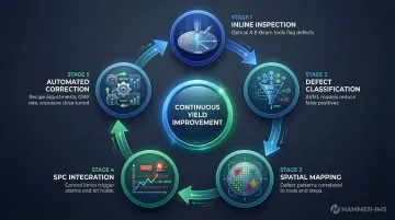
Defect Mapping and Pattern Recognition
Every confirmed defect is plotted on a spatial wafer map. Characteristic spatial patterns reveal root-cause clues:
- Edge-ring clustering: Typically points to CMP, bevel contamination, or plasma non-uniformity
- Center hotspots: Suggest lithography focus or deposition issues
- Repeating array patterns: Across all dies indicate systematic defects tied to mask or reticle degradation
Software like KLA's Klarity automatically detects these spatial defect patterns (rings, edge clusters, scratches). In one case study at Lumileds, Spatial Signature Analysis (SSA) identified a "fish-scale" nuisance defect that formed a distinct ring signature, allowing engineers to filter it out and reveal the true yield-limiting lot-to-lot variations.
Zonal and Statistical Analysis
Fabs divide the wafer into regions—edge vs. center, quadrants, and concentric rings—then calculate defect density per zone. This zonal breakdown supports two complementary analysis methods:
- Density trending: Temporal charts track defect evolution across lots, catching slow process drifts before they escalate into full excursions
- Spatial comparison: Cross-zone benchmarking isolates whether a defect pattern is localized (edge-only) or systemic (wafer-wide), narrowing the root-cause search
Tool and Recipe Correlation
Equipment fingerprinting: when a specific chamber consistently produces higher defect counts or a distinctive defect signature, inspection data points directly to that tool for maintenance or adjustment. Cross-layer correlation links defects in later layers back to earlier process steps, compressing root-cause investigation time.
Tracking the digital fingerprint of tool components—such as the 3D trajectory of a wafer-handling robot—allows fabs to flag deviations before a component fails. Implementing predictive maintenance based on these analytics can save millions; eliminating just one preventive maintenance cycle per year on a high-volume tool can save roughly $21 million in avoided downtime.
Closing the Loop: Automated Triggers and Predictive Control
Inspection data integrates with SPC to define control limits and trigger automated lot holds, alarms, or recipe adjustments. Beyond reactive controls, advanced fabs deploy AI-driven models that forecast tool degradation before defects appear—enabling maintenance to happen on schedule rather than in crisis. The most mature implementations go further, achieving partial closed-loop control that automatically adjusts exposure dose, etch depth, or CMP removal rate based on real-time inspection feedback.
Frequently Asked Questions
What is wafer inspection?
Wafer inspection is the systematic examination of semiconductor wafers using optical, electron beam, and measurement tools to detect surface defects, pattern anomalies, and dimensional irregularities—ensuring only conforming wafers advance through manufacturing.
What is the wafer test process?
The wafer test process (also called wafer sort or probe test) electrically tests each die on a completed wafer to identify passing and failing dies before dicing. This differs from in-process inspection, which occurs continuously throughout manufacturing.
What is the purpose of a wafer?
A semiconductor wafer is the thin silicon disc that serves as the physical substrate on which integrated circuits are built through successive layering, patterning, and etching steps. Its flatness, purity, and dimensional consistency directly affect every subsequent process step.
What is the difference between patterned and non-patterned wafer inspection?
Patterned wafer inspection uses die-to-die or die-to-database comparison to find random and systematic defects within circuit features, while non-patterned (bare) wafer inspection uses laser scattering to detect particles, pits, and crystal defects on unpatterned surfaces.
How does wafer inspection affect semiconductor yield?
Inspection acts as the fab's early-warning system. Catching defects at the earliest possible stage prevents bad wafers from accumulating additional processing cost, and inspection data guides the process corrections that systematically improve yield over time.