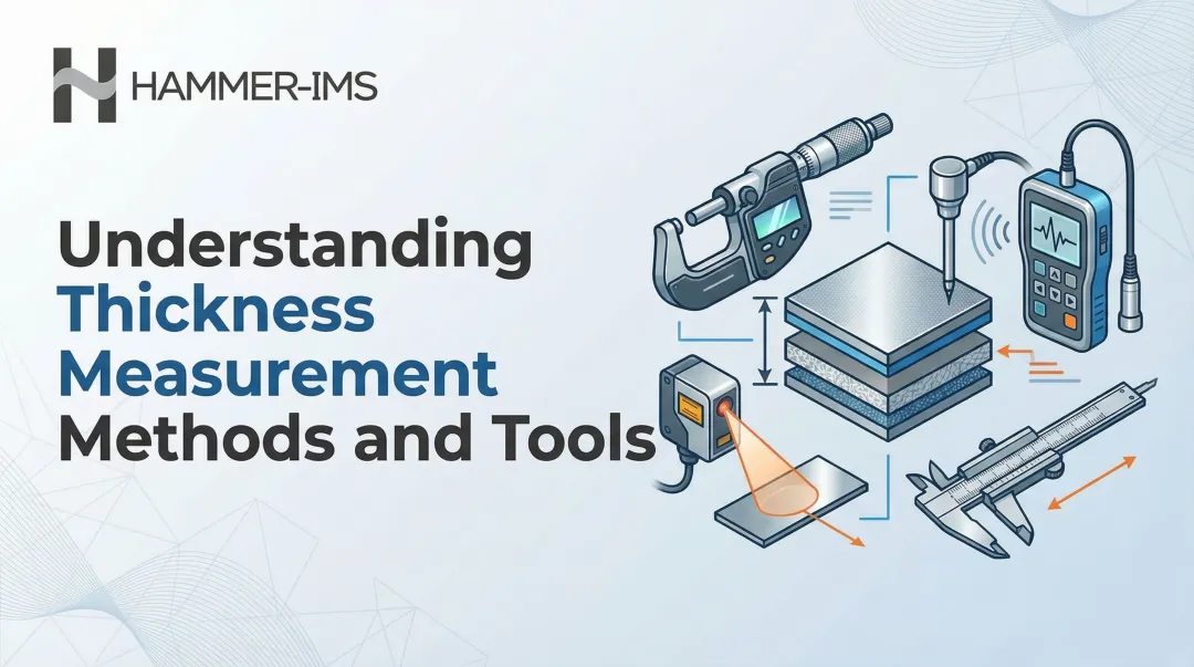
Introduction
In manufacturing, a fraction of a millimetre in thickness deviation can cause yield loss, product failure, or significant material waste. For battery electrode manufacturers, thickness inconsistency contributes approximately 6% to overall battery costs through material scrap alone. In semiconductor fabrication, where High-NA EUV lithography systems operate with a depth of focus as narrow as 40–45 nanometres, even minor wafer thickness variations become catastrophic.
Multiple competing techniques exist — from capacitance probes to interferometry to millimetre wave systems — and no single method suits every application. The right choice hinges on material type, whether contact measurement is feasible, and the precision your process demands. This guide breaks down each technique so you can match the method to your specific production environment.
Key Takeaways
- Wafer thickness measurement ensures dimensional accuracy across semiconductor, plastics, and flat material manufacturing
- Key techniques span capacitance sensing, white light interferometry, laser triangulation, and millimetre wave (M-Ray) technology
- Contact methods risk surface damage; non-contact methods dominate precision inline applications
- The right technique depends on material type (transparent vs. opaque), conductivity, and whether measurement is inline or offline
- Modern inline systems with real-time feedback enable closed-loop process control, reducing waste and thickness variation
What Is Wafer Thickness Measurement and Why It Matters
Wafer thickness measurement is the process of precisely determining how thick a flat or sheet-form material is — semiconductor silicon wafers, plastic films, industrial laminates, nonwoven fabrics — to confirm it meets production specifications. The method varies by material and process, but the underlying need is the same: dimensional control at tolerances that manual gauging cannot reliably achieve.
Where It's Applied
This measurement discipline appears across multiple industries:
- Semiconductor wafer lapping and grinding - Polishing silicon wafers to exact thickness for photolithography
- Thin film extrusion - Controlling plastic film thickness in real-time during production
- Battery electrode coating - Ensuring uniform coating thickness for lithium-ion cell performance
- Medical device film production - Maintaining tight tolerances in thermoplastic extrusion
- Nonwoven fabric manufacturing - Controlling basis weight and thickness for product consistency
Across every one of these applications, the measurement challenges converge on three requirements: uniformity across the full material surface, sensitivity to surface texture or contamination, and speed sufficient for inline or in-process feedback. Those requirements directly shape which metrics manufacturers track.
Key Metrics That Define Quality
Thickness measurement must capture several critical geometric parameters, as defined by ASTM and SEMI standards:
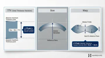
- Total Thickness Variation (TTV) - The difference between maximum and minimum thickness values across the material surface
- Bow - The deviation of the centre point from a reference plane established by three equally spaced points
- Warp - The difference between the maximum and minimum distances of the median surface from a reference plane
For semiconductor wafers, SEMI M1 specifications mandate maximum TTV of 10 µm for 300 mm polished silicon wafers, though advanced applications require tolerances below 1 µm. In battery electrode production, a calender tolerance of ±3.0 μm can cause porosity to vary from 19.6% to 38.6% against a 30% target, requiring massive electrolyte volume adjustments to prevent cell failure.
Major Wafer Thickness Measurement Techniques Explained
Each technique operates on a different physical principle, making it better suited for specific materials, environments, and accuracy levels. Understanding these trade-offs is essential before selecting a system.
Contact Measurement (Mechanical Gauging)
Contact-based methods use physical probes or styluses that touch the wafer surface to measure displacement. They are simple and low-cost but risk surface contamination or scratching, making them unsuitable for polished semiconductor wafers or cleanroom applications. For high-value materials, even microscopic surface damage can compromise downstream processing.
Capacitance-Based Measurement
Capacitance probes detect changes in the electrical gap between the probe face and the target surface. A push-pull dual probe arrangement—with one sensor on each side of the wafer—cancels out surface irregularities and bow to deliver true thickness readings.
Push-pull capacitance designs use a 180-degree phase shift to route current across the target surface instead of to ground, eliminating inaccuracies on poorly grounded or highly resistive targets. This makes them reliable for electrically conductive materials. That said, varying target resistivity can introduce measurement error without proper compensation design.
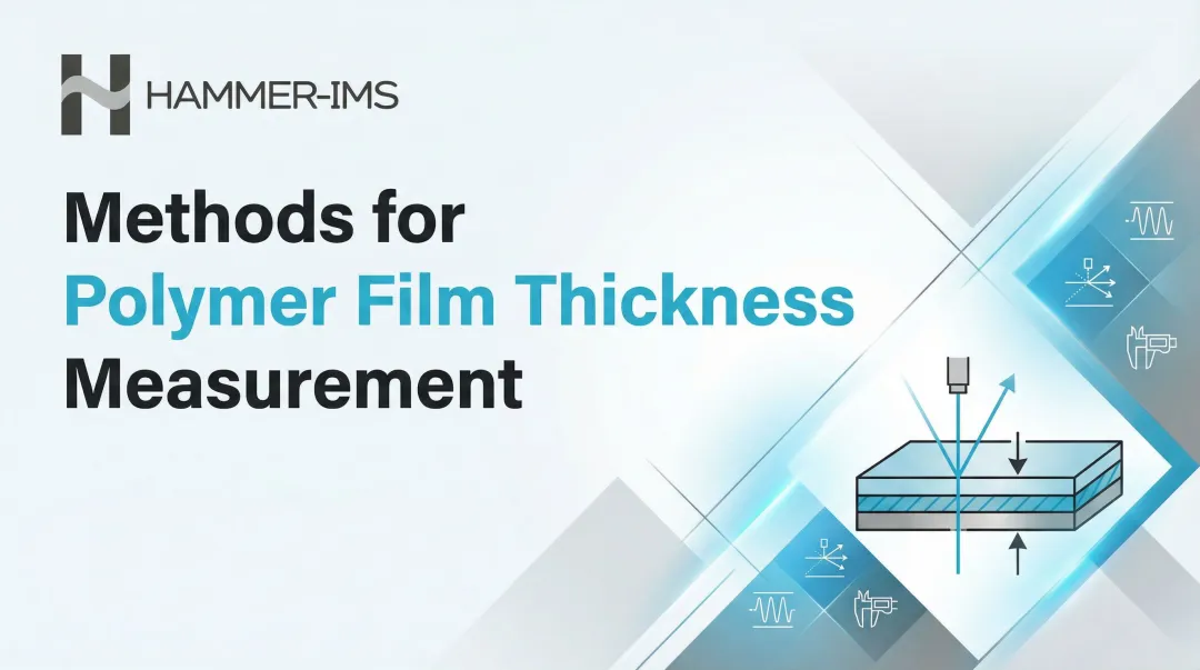
White Light and IR Interferometry
Interferometric methods use a split light beam reflected from the front and back surfaces of a transparent or semi-transparent material. White light interferometers using superluminescent diodes (SLDs) achieve nanometre-level accuracy and are particularly effective for silicon wafers in lapping machines and cleanroom environments.
Silicon is optically transparent at wavelengths beyond approximately 1,100 nm, enabling near-infrared interferometry. Axial resolution depends on the source's coherence length—a function of central wavelength and spectral bandwidth.
One firm constraint applies: the material must be optically transparent in the relevant wavelength range. Opaque or heavily absorbing materials fall outside this method's reach.
Laser Triangulation
Laser triangulation sensors project a laser spot or line onto the material surface and calculate thickness from the reflected angle. Commercial systems achieve sampling speeds up to 392 kHz, making them suited for opaque materials and offering excellent inline speed.
However, they struggle with highly reflective or transparent surfaces due to speckle noise, and factors such as local surface slope, roughness, and illumination changes degrade accuracy.
Millimetre Wave (M-Ray) Technology
Millimetre wave-based systems transmit and receive electromagnetic waves in the millimetre frequency range (30–300 GHz) to measure thickness contactlessly. FMCW radar systems measure the time delay between reflections at material interfaces, calculating absolute layer thickness from transit time differences when the material's refractive index is known.
This technology requires no optical transparency or electrical conductivity—making it effective for plastics, foams, nonwovens, and composite sheets. For inline production environments handling these materials, it offers contactless operation, no radiation hazard, and measurement speeds suited to continuous process lines.
Comparing Techniques: How to Choose the Right One for Your Application
The "best" technique depends on a combination of material properties, production environment, accuracy requirements, and operational constraints.
Material Properties Drive Technique Selection
Material type is the first filter. A quick guide:
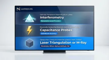
- Optically transparent materials (silicon, glass films): interferometry exploits light transmission to achieve nanometre-level precision — the standard for semiconductor applications
- Electrically conductive materials (metals, silicon wafers): capacitance probes measure the electrical gap between probe and surface, delivering sub-micron accuracy
- Opaque, non-conductive materials (plastics, foam, textiles): laser triangulation handles moderate reflectivity well; millimetre wave penetrates materials where optical methods fail entirely
Environment and Integration Requirements
The production environment narrows the choice further:
- Cleanroom and vacuum environments: require IP-rated or vacuum-compatible sensors with no particle generation — non-negotiable in semiconductor manufacturing
- High-speed inline lines: need fast sampling rates and real-time output; plastic film extrusion lines, for instance, require continuous measurement across the full web width without slowing production
- Offline quality labs: prioritise absolute accuracy over speed, making time-intensive techniques like interferometry with multiple measurement passes a viable option
Accuracy Tiers and Their Implications
Nanometre-level TTV requirements — common in semiconductor photolithography — typically require interferometry. When depth of focus shrinks to 40–45 nm in High-NA EUV systems, residual wafer topography and TTV directly cause defocus, leading to pattern collapse and yield loss.
Micron-range tolerance control, as found in plastic film extrusion, can be served by laser or millimetre wave systems. ASTM D8136 standardises the measurement of plastic film thickness variability (2.5 to 250 µm) using non-contact capacitance gauges to profile transverse and machine directions.
Safety and Regulatory Considerations
Regulatory compliance is a technique constraint in its own right. Some facilities still run nuclear (beta/gamma) gauges, but the overhead is significant. US NRC 10 CFR 32.31 requires manufacturers to demonstrate that devices will not expose individuals to doses exceeding 200 µSv annually, with strict labelling and disposal requirements. In Europe, Council Directive 2013/59/Euratom sets binding basic safety standards for protection against ionising radiation.
These compliance, training, and disposal costs are accelerating the shift toward non-nuclear alternatives — particularly millimetre wave and laser systems.
Practical Selection Framework
| Material Type | Transparency | Conductivity | Recommended Technique |
|---|---|---|---|
| Silicon wafer | Transparent (>1100 nm) | Conductive | Interferometry or capacitance |
| Plastic film | Opaque or semi-transparent | Non-conductive | Laser triangulation or M-Ray |
| Metal sheet | Opaque | Conductive | Capacitance |
| Foam | Opaque | Non-conductive | M-Ray or laser triangulation |
| Nonwoven fabric | Opaque | Non-conductive | M-Ray |
Wafer Thickness Measurement in Practice – A Step-by-Step Example
The techniques described above come together clearly in a practical scenario. Consider a plastic film production line that needs to tighten thickness consistency across a wide web of extruded material to reduce waste and improve product uniformity. Here's how an inline non-contact measurement system gets selected, installed, and integrated from start to finish.
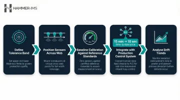
Stage 1: Define Measurement Objective and Tolerance Band
Establish the target thickness range (e.g., 250 µm ± 5 µm) and identify the acceptable variation across the web width. Determine whether the goal is to reduce scrap, improve product performance, or meet customer specifications.
What commonly goes wrong: Skipping this step and deploying sensors without clear targets. The result is data collection without any actionable process improvement — measurements that inform nobody.
Stage 2: Select and Position Sensors Across the Web Profile
Choose a non-contact technique appropriate for the material (millimetre wave for opaque plastic films). Position multiple sensors or a scanning head to cover the full web width, not just the centre.
What commonly goes wrong: Positioning sensors only at the centre of the web rather than across the full profile, missing edge effects and creating blind spots where thickness deviations go undetected.
Stage 3: Take Baseline Measurements and Calibrate Against Known Reference Standards
Run production material through the measurement system and compare readings against calibrated reference standards. Adjust sensor parameters to eliminate offset errors and ensure accuracy.
What commonly goes wrong: Skipping material-specific calibration and assuming factory settings are accurate. Systematic offset errors then compound quietly across every production run.
Stage 4: Connect Measurement Output to the Production Control System
Integrate sensor data with the production control system (PLC or SCADA) for real-time adjustment. Configure automated feedback loops that adjust die bolts, haul-off speed, or pump flow rates to maintain target thickness.
One published case study combining an NDC scanning system with a Prodigi motorised lip actuator cut time-to-tolerance from 15 minutes (using thermal bolts) down to 10 seconds, reaching flat film within 30 seconds of startup.
What commonly goes wrong: Failing to integrate sensor data with the production control system, leaving measurement as a passive quality check rather than an active production tool.
Stage 5: Review Measurement Logs to Identify Thickness Drift Trends
Analyse historical thickness data to identify patterns and proactively intervene. Track trends over hours, shifts, or production runs to detect gradual die wear, temperature drift, or material property changes.
What commonly goes wrong: Treating measurement data as purely transactional — pass or fail in the moment. A few common pitfalls with this approach:
- Gradual die wear goes unnoticed until scrap rates spike
- Temperature drift accumulates across shifts without triggering any alert
- Material property changes between batches are attributed to equipment faults instead of incoming material variation
How Hammer-IMS Can Help
Hammer-IMS provides non-nuclear, contactless thickness measurement solutions built around M-Ray millimetre wave technology. The systems are designed for industrial producers of plastic films, nonwovens, foams, composites, and other flat materials that require precise inline thickness control without the regulatory burden of nuclear gauges.
Key Differentiators
- M-Ray contactless measurement operates at 60 GHz using a transmission-reflection approach, measuring through opaque and coloured materials where optical systems fail
- Closed-loop production control via Connectivity 3.0 software adjusts bolt power, line speed, and pump flow in real time to hold thickness within tolerance
- Drift detection and analytics log thickness data continuously, letting manufacturers intervene early before scrap accumulates
- Full cross-web coverage through multiple sensors with lateral scanning capability maps local highs and lows across 100% of the production web, directly reducing material waste
For manufacturers evaluating alternatives to nuclear gauge systems, Hammer-IMS offers a non-radioactive option that integrates into existing production infrastructure via Modbus TCP/IP, OPC UA, and PROFINET protocols.
Frequently Asked Questions
What is total thickness variation (TTV) and why does it matter in wafer manufacturing?
TTV is the difference between maximum and minimum thickness across a wafer or flat material surface. High TTV causes downstream defects—such as focus errors in photolithography or non-uniform coating in film production—directly impacting yield and product performance.
What is the difference between contact and non-contact wafer thickness measurement?
Contact methods physically touch the surface to measure displacement, risking surface damage and contamination. Non-contact methods use capacitance, optical, or electromagnetic techniques to measure without touching, making them preferred for polished, fragile, or contamination-sensitive materials.
How does capacitance-based wafer thickness measurement work?
A capacitance probe measures changes in the electrical gap between probe and surface. Placing probes on both sides of the wafer in a dual push-pull arrangement cancels bow and warp effects, delivering a true thickness reading. Accuracy can still be affected by variations in target resistivity.
Can wafer thickness be measured inline during the production process?
Yes, modern non-contact systems (laser, interferometric, and millimetre wave) are designed for inline use, providing continuous real-time thickness data that feeds back to production controls—enabling closed-loop process adjustment without stopping production.
What factors most affect the accuracy of a wafer thickness measurement system?
The primary accuracy-influencing factors are:
- Material optical or electrical properties
- Surface finish and cleanliness
- Vibration in the measurement environment
- Sensor calibration quality
- Compensation for bow and warp
Why are non-nuclear thickness measurement techniques gaining preference in industrial applications?
Nuclear (beta/gamma) gauges require strict regulatory compliance, specialised handling, and ongoing licensing costs. Non-nuclear alternatives — laser, interferometric, and millimetre wave systems — offer comparable or superior accuracy with none of these constraints, removing the main barriers to adoption in regulated and safety-sensitive environments.