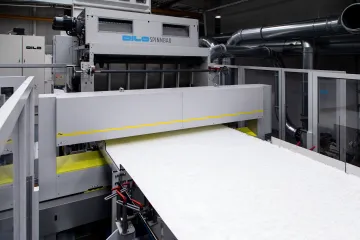
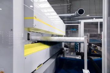
Semiconductor Inspection Solutions and Applications

Hammer-IMS delivers cutting-edge, non-nuclear semiconductor inspection solutions powered by advanced M-Ray millimeter wave technology. From contactless thickness measurement to inline quality control, our systems provide real-time, high-precision data that helps semiconductor and electronics manufacturers reduce defects, minimize material waste, and maintain exacting production standards — all with a clean, safe, and scalable measurement platform.

Advanced semiconductor inspection system using millimeter wave technology for contactless measurement

Our Semiconductor Inspection Solutions Services

Explore our range of non-nuclear, contactless measurement and inspection technologies designed for precision semiconductor and advanced materials quality control.

M-Ray Technology

Multifunctional millimeter wave technology enabling contactless dimensional measurement, material characterization, and displacement measurement at multiple kHz rates — ideal for highly dynamic semiconductor production environments requiring clean, invisible sensing.

M-Ray OEM Module

A compact, non-nuclear OEM measurement module designed for integration into semiconductor equipment, inline quality systems, or research platforms — providing thickness and basis-weight measurement with a small form factor and full API support.

Marveloc 602 Platform

An affordable, high-performance millimeter wave measurement platform for clean and contactless thickness and basis-weight inspection of flat materials, available as an OEM version for system integrators and semiconductor equipment partners.

Clean Measurement Technology

Precise, Non-Nuclear Inspection Built for Advanced Manufacturing

Hammer-IMS's M-Ray millimeter wave technology brings a new standard to semiconductor and advanced materials inspection. Operating entirely without radioactive sources, our contactless systems deliver real-time thickness, basis-weight, and material characterization data at measurement rates up to multiple kHz — fast enough for high-speed production lines. Whether integrated as an OEM module or deployed as a turn-key inline system, Hammer-IMS solutions support closed-loop process control, reduce material waste, and ensure uniform product quality across every production run.

Contactless M-Ray sensor performing thickness inspection on a flat semiconductor material
Trusted By Industry Leaders

Success Stories

See how leading manufacturers worldwide rely on Hammer-IMS measurement technology to achieve production excellence.

"Sustainability is always a consideration for us. In our search for alternatives to radioactive source machines, we discovered the remarkable flexibility of Hammer-IMS. These solutions not only align with our objectives but also aid in crafting personalized, tailored solutions to fit our needs."

Jo Cinjaere
Jo Cinjaere
The Hammer-IMS Difference

Why Choose Hammer-IMS?

Hammer-IMS combines deep measurement science expertise with an unwavering commitment to clean, safe, and innovative inspection technology.

Non-Nuclear Safety

Our M-Ray technology is entirely non-radioactive, enabling safe 24/7 operation by personnel without regulatory restrictions.

Global Reach

With service presence across Europe, Australia, Japan, and North America, Hammer-IMS supports your operations wherever they run.

Real-Time Control

Closed-loop production feedback and data analytics integration allow immediate process adjustments, reducing defect rates and material waste.

Scalable Integration

From compact OEM modules to full turn-key inline systems, our solutions scale seamlessly into existing semiconductor production equipment.

The Hammer-IMS Team

A dedicated team of measurement technology experts driving innovation in industrial quality control.

Hammer-IMS develops and delivers innovative, high-tech quality and process control solutions for industries worldwide, with a sharp focus on non-nuclear measurement technologies. Our team combines deep expertise in millimeter wave physics, industrial automation, and software engineering to create systems that are both powerful and practical. With strategic international partnerships — including our recent expansion into Japan through collaboration with ADSTEC — and a branch in Spartanburg serving North American customers, Hammer-IMS has built a global footprint grounded in local support. We are driven by a mission to maximize production efficiency, reduce waste, and make accurate, non-destructive inspection the global manufacturing standard.

20+ Industries ServedTrusted across textiles, plastics, construction, automotive, medical, and advanced materials sectors.
Multi-kHz MeasurementMeasurement rates supporting production line speeds of up to 500 meters per minute.
Global Service NetworkActive support across Belgium, Germany, France, Netherlands, Australia, Japan, and North America.

Frequently Asked Questions

What is semiconductor inspection?

Semiconductor inspection is the process of detecting defects, measuring dimensions, and verifying material properties in semiconductor materials and devices during or after manufacturing. It encompasses techniques like contactless thickness measurement, surface defect detection, and material characterization to ensure that wafers, films, and substrates meet precise quality and dimensional specifications before advancing through the production process.

What are the 4 types of inspection?

How does M-Ray millimeter wave technology work for semiconductor inspection?

Is M-Ray technology safe for continuous production environments?

Can the M-Ray OEM Module be integrated into existing semiconductor equipment?

What measurement accuracy can be expected from Hammer-IMS inspection systems?

Do you offer turn-key inspection system installations?

How can I evaluate whether Hammer-IMS technology suits my semiconductor application?

Still Have Questions About Our Inspection Solutions?

Speak with a Hammer-IMS measurement specialist for a no-obligation technical consultation.

Our Global Service Areas

Hammer-IMS delivers inspection solutions and on-site support to manufacturers across Europe, Asia-Pacific, and North America.

6+ Countries

Service Regions

Mon–Fri, 8:30AM–5:30PM

Availability

Spartanburg, SC

North America Branch

Do We Service Your Region?

Contact our international or North America team to confirm coverage and schedule your consultation.

Certified & Trusted

Awards and Recognition

Non-nuclear compliance certification badge for Hammer-IMS M-Ray technology

Non-Nuclear Compliance

Certified non-radioactive technology safe for unrestricted industrial use.

Industry 4.0 compatibility certification logo for Hammer-IMS IoT measurement platform

Industry 4.0 Ready

Certified IoT and Industry 4.0 compatible measurement and analytics platform.

ISO quality management standard certification logo for Hammer-IMS

Quality Assurance Standard

Adherence to international quality management and process control standards.

Get a Tailored Semiconductor Inspection Consultation

Tell us about your application, material type, and production requirements. Our measurement engineers will recommend the right M-Ray inspection configuration and arrange a live demonstration at your convenience.

Contact Us Today

For immediate assistance, feel free to give us a direct call at +32 11 36 55 01.