Surface quality is one of the most visible indicators of manufacturing precision. Whether it’s the finish on an aerospace component, the coating on a medical device, or the texture of an automotive body panel, even minor imperfections can signal deeper issues in a production process.
This is why manufacturers across are shifting toward optical surface inspection, systems capable of detecting microscopic defects at high speed and with consistent accuracy.
Recent data shows how rapidly this shift is accelerating. The Automated Optical Inspection (AOI) market is expected to reach $2.07 billion in 2026, driven by the widespread adoption of smart manufacturing and AI-enabled inspection tools.
As optical methods evolve, from 2D/3D vision to laser triangulation, structured light, and photometric stereo, they’re becoming central to quality assurance strategies. The following guide breaks down these technologies and explains how manufacturers can use them for more reliable, data-driven inspection.
TL;DR
Optical surface inspection detects scratches, dents, pits, coating flaws, and contamination faster and more accurately than manual methods.
Key technologies include 2D/3D vision, laser triangulation, structured light, confocal microscopy, photometric stereo, and hyperspectral imaging.
Inline systems provide real-time monitoring, while offline setups offer ultra-high-resolution analysis for prototypes or critical parts.
Success depends on KPIs such as accuracy, repeatability, defect detection rate, and traceable data management for regulatory compliance.
Advanced solutions with AI-driven analysis and integrated software reduce scrap, improve traceability, and enhance overall production quality.
What Is Optical Surface Inspection?
Optical surface inspection refers to the use of cameras, sensors, lasers, and lighting systems to evaluate a product’s exterior for defects, deviations, or irregularities, without any physical contact.
Instead of relying on human inspectors or tactile measurement tools, these systems capture high-resolution images or 3D surface profiles and analyze them using algorithms or AI models to detect issues such as scratches, dents, pits, burrs, coating flaws, or contamination.
At its core, optical inspection converts visible or reflected light into measurable data. This allows manufacturers to verify surface quality with much greater consistency, speed, and accuracy than manual methods.
Optical systems can be configured as:
2D machine vision setups for detecting contrast-based defects
3D vision systems using structured light or laser triangulation
Microscopy or interferometry systems for sub-micron precision
Inline inspection stations synchronized with automated production lines
Because the process is non-contact and extremely fast, it supports real-time quality assurance, reduces human variability, and provides digital traceability, requirements that have become standard across automotive, aerospace, electronics, and medical-device manufacturing.
Core Optical Surface Inspection Technologies
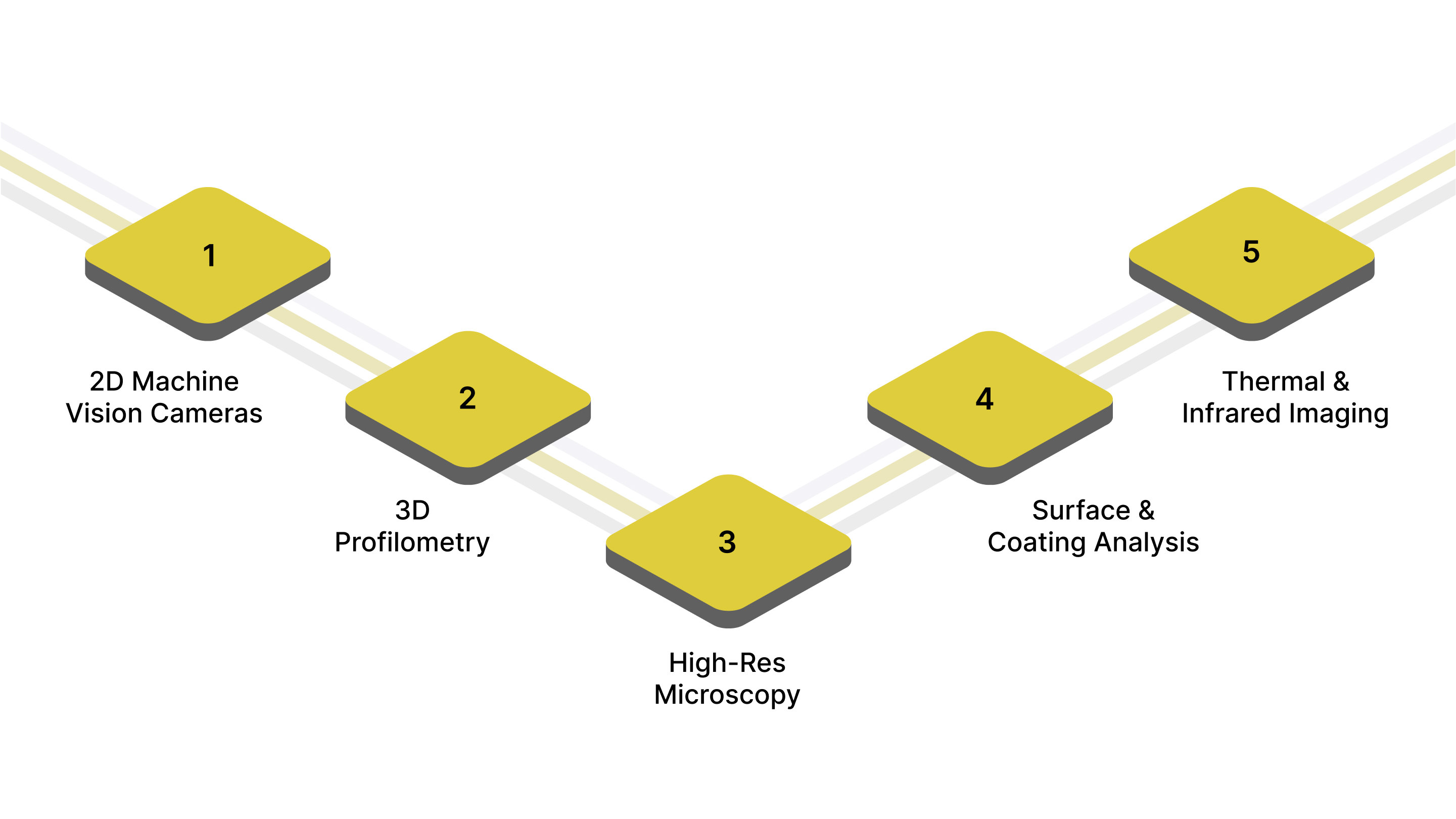
Optical surface inspection relies on a variety of imaging and sensing technologies, each suited to specific defect types, materials, and precision requirements. These can be grouped into 2D vision, 3D profilometry, high-resolution microscopy, and advanced spectral/thermal methods.
1. 2D Machine Vision Cameras
High-resolution area-scan or line-scan cameras capture surface images under controlled lighting. These systems are ideal for detecting visible defects such as scratches, stains, and missing features on flat or moderately contoured surfaces.
They are widely used in high-speed inline inspections across automotive panels, electronics casings, and consumer products.
2. 3D Profilometry: Laser Triangulation and Structured Light
Laser triangulation projects a laser line onto a surface and measures deformations to create a 3D profile, making it perfect for identifying dents, weld bead irregularities, and edge features. Structured light systems project known patterns, such as stripes or grids, onto surfaces and analyze distortions to reconstruct complex geometries.
These methods are especially useful for automotive body panels, aerospace components, and freeform surfaces.
3. High-Resolution Microscopy: Confocal and White Light Interferometry
Confocal microscopy focuses light at varying depths to produce ultra-fine surface measurements, suitable for micro-textures, micro-cracks, and roughness in medical implants, microelectronics, and semiconductor components.
White light interferometry (WLI) uses interference patterns from split beams to measure nanometer-scale roughness, making it ideal for precision optics and semiconductor wafers.
4. Surface Texture and Coating Analysis: Photometric Stereo and Hyperspectral Imaging
Photometric stereo captures multiple images under different lighting angles to reveal subtle texture variations, ideal for low-contrast defects, matte surfaces, or painted parts. Hyperspectral and multispectral imaging detect variations across many wavelengths, allowing inspection for material inconsistencies, contamination, and coating or film thickness defects.
5. Thermal and Infrared Imaging
Infrared and thermal cameras identify subsurface defects by detecting heat signatures or thermal conductivity changes. These systems are often applied to composite parts, electronics assemblies, and plastic injection-molded components where subsurface or hidden defects can affect performance.
By presenting these technologies in grouped, paragraph form, manufacturers can more easily match inspection methods to their part geometries, materials, and defect detection requirements.
Inline vs. Offline Surface Inspection
Choosing between inline and offline inspection depends on production volume, accuracy requirements, and how quickly defects need to be identified.
Feature / Criteria | Inline Surface Inspection | Offline Surface Inspection |
|---|---|---|
Purpose | Real-time defect detection during production | High-precision analysis outside the production line |
Speed | Very high; synchronized with cycle time | Moderate; depends on operator and equipment setup |
Accuracy | High but optimized for speed | Very high; supports micro- and nano-level resolution |
Typical Use Cases | Automotive assembly lines, electronics manufacturing, packaging, and metal fabrication | R&D labs, quality labs, first-article inspection, root-cause analysis |
System Complexity | Complex integration with conveyors, robots, and PLCs | Standalone systems; easier setup |
Data Output | Continuous inspection data, supports SPC and trend monitoring | Detailed surface maps, 3D profiles, roughness/texture analysis |
Cost | Higher initial investment due to automation | Lower upfront cost; higher per-part-time cost |
Operator Involvement | Minimal—automated | Moderate; requires handling and positioning |
Flexibility | Limited; designed for specific parts | Highly flexible for multiple part types and geometries |
Environment | Must withstand vibration, dust, and temperature changes | Controlled environment; stable lighting and vibration isolation |
Best For | High-volume manufacturing requiring consistent throughput | Precision-critical components, prototypes, and failure investigation |
Key Performance Metrics (KPIs)
Measuring the effectiveness of an optical surface inspection system requires tracking metrics that reflect accuracy, reliability, and production efficiency. Manufacturers often rely on the following KPIs to ensure consistent quality and return on investment:
Accuracy: Degree to which measurements reflect the true surface geometry.
Repeatability & Reproducibility (R&R): Ability to consistently produce the same measurement results under identical conditions.
Resolution: Smallest defect or surface variation the system can detect.
Throughput / Cycle Time: Number of parts inspected per unit time.
Uptime / Availability: Percentage of operational time versus downtime.
False Accept / False Reject Rate: Rate of incorrectly passing defective parts or rejecting good parts.
Measurement Uncertainty: Quantifies the confidence level in each measurement.
Process Capability (Cp, Cpk): Statistical measure of how well a process produces parts within specification limits.
Defect Detection Rate (DDR): Percentage of defects correctly identified.
Data Integration & Traceability: Ability to record, store, and analyze inspection data.
Common Defects Optical Systems Detect
Optical surface inspection systems are designed to identify a wide range of defects, from visible scratches to subtle surface irregularities, that can impact product quality, regulatory compliance, and customer satisfaction. Here are the most common defects detected across U.S. manufacturing industries:
Defect Type | Description | Typical Applications / Examples |
|---|---|---|
Scratches & Abrasions | Surface marks caused by handling, machining, or tooling | Automotive body panels, electronics casings, and medical instruments |
Dents & Dings | Depressions or impact damage on a surface | Metal stamping, aerospace components, consumer appliances |
Pits & Porosity | Small holes or voids, often due to casting, welding, or coatings | Aerospace parts, metal castings, plastic molds |
Burrs & Sharp Edges | Excess material left after cutting, stamping, or machining | Mechanical components, electronics housings |
Coating & Paint Defects | Uneven coating, peeling, discoloration, or runs | Automotive painting, medical device coatings, consumer products |
Surface Roughness / Waviness | Deviations from intended smoothness or flatness | Precision optics, machined metal parts, semiconductor wafers |
Contamination / Foreign Particles | Dust, fibers, oil, or debris adhering to the surface | Electronics assemblies, medical devices, and cleanroom manufacturing |
Weld / Solder Defects | Cracks, incomplete fusion, or irregular bead formation | Automotive assemblies, aerospace frames, PCB boards |
Dimensional Deviations | Surface features outside tolerance (height, curvature, spacing) | Aerospace, automotive, and industrial machined parts |
Micro-Cracks & Subsurface Defects | Tiny fissures not visible to the naked eye | Semiconductor wafers, glass surfaces, and high-stress mechanical components |
Implementing an Optical Inspection System
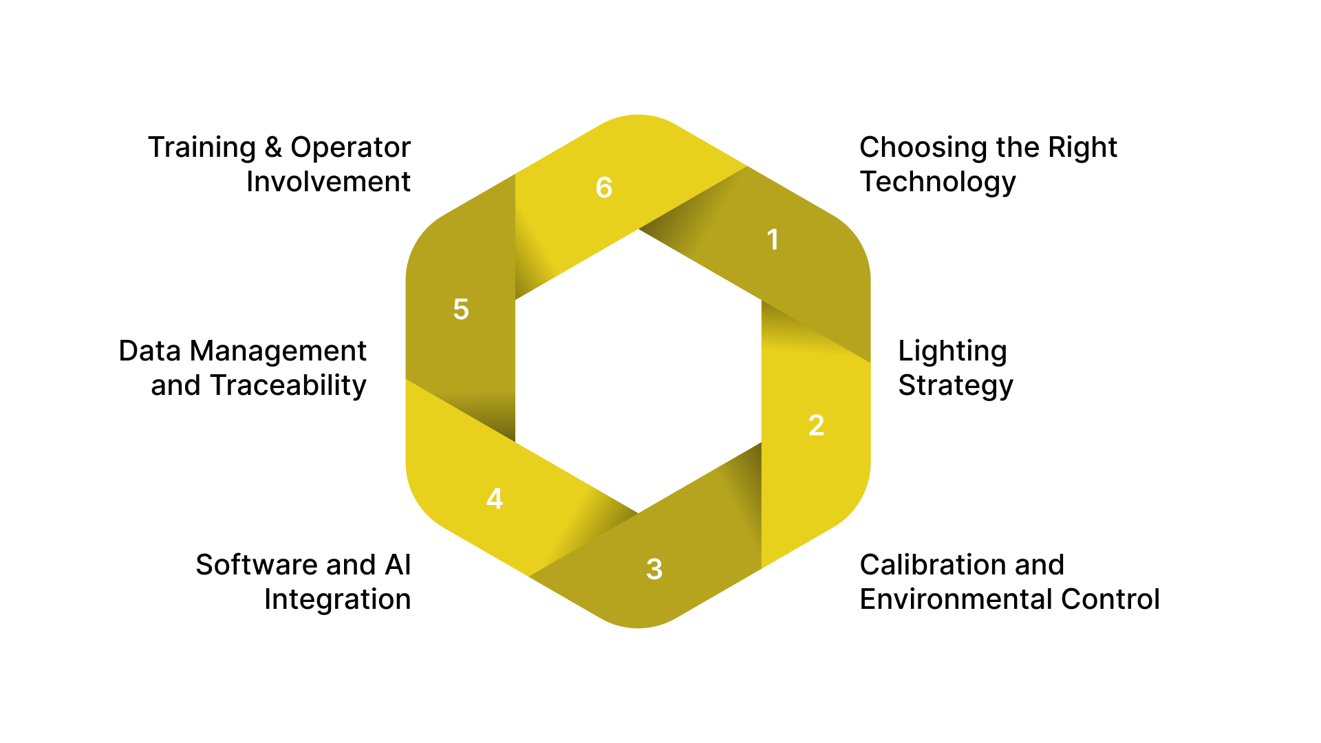
Successfully implementing an optical surface inspection system involves more than just installing cameras or sensors. Manufacturers must carefully consider system selection, integration, calibration, and data management to ensure consistent, high-quality results.
1. Choosing the Right Technology
The first step is selecting an inspection method that aligns with the part geometry, material, and required defect detection sensitivity. For example, 2D machine vision may be sufficient for detecting scratches or paint defects, while laser triangulation or structured light is better for complex 3D surfaces. High-precision applications, such as semiconductor wafers or medical implants, may require confocal microscopy or white light interferometry.
2. Lighting Strategy
Lighting is one of the most critical factors for effective optical inspection. Techniques such as backlighting, coaxial lighting, diffuse dome lighting, or ring lights can dramatically improve defect visibility. Different materials and surface finishes may require customized lighting setups to reduce glare, shadows, and reflections.
3. Calibration and Environmental Control
Regular calibration ensures that the system maintains accuracy and repeatability. Environmental factors like vibration, temperature fluctuations, and dust can affect measurement quality, especially for high-resolution 3D or interferometric systems. Many U.S. manufacturers implement vibration isolation tables, temperature-controlled enclosures, and cleanroom conditions for sensitive inspection tasks.
4. Software and AI Integration
Modern optical inspection systems often include AI or machine learning capabilities to classify defects, detect patterns, and distinguish between acceptable variations and true defects. Software integration allows for seamless data flow into existing quality management systems (QMS), statistical process control (SPC) dashboards, and production reporting tools, enabling real-time decision-making and process optimization.
5. Data Management and Traceability
Digital record-keeping is essential for compliance with U.S. regulatory standards, including FDA, aerospace quality requirements. Storing inspection data securely, either on-premises or in the cloud, allows manufacturers to track defect trends, support root-cause analysis, and maintain traceability for audits and certifications.
6. Training and Operator Involvement
Even automated systems require trained personnel to configure inspection parameters, monitor system performance, and interpret data. A well-trained team ensures the system operates optimally and that defect detection thresholds are correctly adjusted for evolving production conditions.
Advantages and Limitations of Optical Inspection
Understanding both the strengths and constraints of optical inspection systems helps manufacturers make informed decisions, ensuring the chosen solution aligns with production goals, part complexity, and budget.
Aspect | Advantages | Limitations |
|---|---|---|
Accuracy & Precision | High-resolution measurements detect micro-level defects | May require controlled environments for ultra-precise measurements |
Speed & Throughput | Fast inspection; suitable for high-volume production lines | High-speed systems may compromise ultra-fine resolution |
Non-Contact Inspection | No risk of damaging delicate parts | Reflective or transparent surfaces can be challenging |
Consistency & Repeatability | Reduces human error and variability | Requires proper calibration and maintenance to maintain performance |
Automation & Integration | Can be integrated with PLCs, MES, and SPC systems | Higher upfront integration costs and complexity |
Data & Traceability | Provides digital records for regulatory compliance | Large data volumes require robust storage and analysis systems |
Flexibility | Capable of inspecting various defect types and materials | Some systems are optimized for specific part shapes or sizes |
Cost Efficiency (Long-Term) | Reduces scrap, rework, and labor costs over time | High initial investment |
Future Trends in Optical Surface Inspection
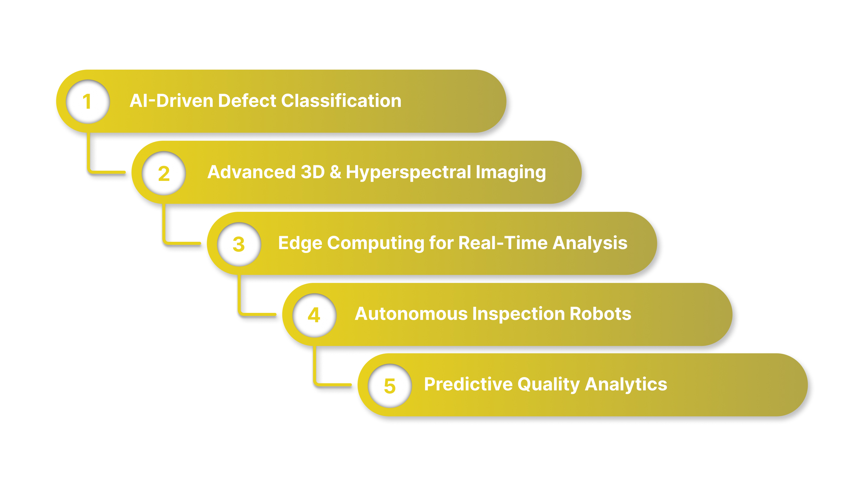
Optical surface inspection is advancing quickly as U.S. manufacturers adopt new AI, imaging, and automation technologies to improve quality and reduce downtime. Key trends include:
AI-Driven Defect Classification: Machine learning models now distinguish normal variations from true defects with greater accuracy, reducing false rejects and improving efficiency.
Advanced 3D and Hyperspectral Imaging: High-resolution 3D and hyperspectral systems capture richer data, enabling detection of subtle irregularities, material inconsistencies, and subsurface defects—even on reflective or multilayered surfaces.
Edge Computing for Real-Time Analysis: Moving data processing to the edge lowers latency and supports immediate quality decisions in high-volume production environments.
Autonomous Inspection Robots: Mobile robotic platforms perform consistent, operator-free inspections of large or complex assemblies, reaching areas traditional systems can’t.
Predictive Quality Analytics: Combining inspection data with process insights helps identify emerging quality issues early, supporting proactive improvements and reducing scrap.
Why Hammer‑IMS Matters for Optical Surface Inspection
If you are looking to implement or upgrade optical surface inspection (or inline quality measurement) in industrial production, Hammer‑IMS offers a compelling example of how advanced inspection technologies are applied in practice.
Non‑contact & Non‑nuclear: Because Hammer‑IMS avoids radioactive sources, their systems are safer, more environmentally friendly, and easier to integrate, aligning with modern industry and regulatory expectations.
Versatility across Materials & Industries: Their offerings support a wide variety of materials, from nonwovens, textiles, plastics, films, composite sheets, to battery films, showing how optical and sensor-based inspection can adapt to different production contexts.
Inline & Real‑Time Monitoring: Hammer‑IMS systems are designed for inline quality control, providing continuous measurements (thickness, basis-weight) or real-time surface inspections, making them representative of how optical inspection can support production without causing bottlenecks.
Integrated Software & Data Connectivity: Their “Connectivity 3.0” software enables unified control and integration of measurement/inspection data, important for process traceability, SPC (Statistical Process Control), and integration with existing manufacturing workflows.
Hammer‑IMS offers ready‑to-deploy systems that align with best practices in optical inspection, process control, and regulatory compliance. Book a demo today.
Conclusion
Whether integrated inline for real-time production monitoring or employed offline for high-precision lab analysis, these systems support critical quality metrics, reduce scrap, and provide traceable data for regulatory compliance. While optical inspection offers significant advantages, such as non-contact measurement, automation, and data-driven insights, manufacturers must also account for environmental factors, system calibration, and initial investment costs.
For U.S. manufacturers across automotive, aerospace, electronics, and medical-device industries, investing in robust optical surface inspection methods is no longer optional. It is a strategic imperative to maintain competitive advantage, ensure regulatory compliance, and consistently deliver products that meet the highest standards of quality.
Take action today and elevate your manufacturing quality with advanced optical surface inspection solutions.
Whether you’re aiming to reduce scrap, ensure regulatory compliance, or achieve zero-defect production, investing in modern inspection technologies can give your operations a measurable edge.
Contact Hammer‑IMS or your preferred optical inspection provider today to explore systems tailored to your production needs, schedule a demo, or receive a consultation on integrating inline or offline inspection into your facility. Ensure your products meet the highest quality standards, every time.
FAQs
1. Can optical inspection detect internal defects?
While primarily designed for surface evaluation, some advanced methods like infrared or thermal imaging can identify near-surface defects, but truly internal defects may require complementary techniques such as X-ray or ultrasonic inspection.
2. How do optical inspection systems handle reflective or transparent materials?
Highly reflective or transparent surfaces can pose challenges. Solutions include using polarized lighting, diffused illumination, or specialized imaging techniques like structured light or interferometry to minimize glare and enhance defect visibility.
3. Are optical inspection systems suitable for small-scale manufacturers?
Yes. Sensor miniaturization, AI-driven analysis, and lower-cost vision systems make optical inspection accessible to small and mid-sized manufacturers, allowing them to maintain high-quality standards without large-scale infrastructure.
4. How frequently should optical inspection systems be calibrated?
Calibration frequency depends on the precision requirements and usage intensity. Critical applications, like medical devices or aerospace components, often require monthly or even weekly calibration, while less critical inspections may be quarterly.
5. Can optical inspection systems integrate with other quality control tools?
Absolutely. They can feed data into SPC dashboards, ERP systems, and automated production lines, allowing manufacturers to track trends, trigger alerts, and link inspection results with process parameters for continuous improvement.
6. How does AI improve defect detection over traditional imaging?
AI can classify subtle or complex defects that conventional rule-based algorithms might miss. It also adapts to variations in part geometry, lighting, and materials, reducing false positives and improving overall inspection reliability.
7. What industries benefit the most from optical inspection outside of automotive and aerospace?
Other industries include consumer electronics (PCB and device casing inspection), medical devices (implant surfaces, surgical instruments), and precision optics (lens and mirror surfaces), where micro-level surface quality is critical.