Introduction
A measurement system that drifts out of calibration mid-shift, or degrades silently until defects reach the customer, isn't a quality tool — it's a liability. For industrial manufacturers, this gap between expected and actual sensor performance is where production losses quietly accumulate.
Digital X-ray sensor technology has become foundational in industrial non-destructive testing (NDT) and process measurement. Image quality, detection sensitivity, and operating reliability directly determine whether measurements translate into real quality control or just data overhead.
What datasheets promise and what sensors deliver on the production floor are often two different things. Understanding sensor architecture, performance parameters, and operating boundaries is essential for correct selection, system integration, and reliable deployment.
For manufacturers in plastic extrusion, nonwovens, textiles, and similar continuous-web processes, the operational reality of X-ray sensing frequently includes radiation safety compliance and material sensitivity constraints that add complexity well beyond the measurement itself. This article breaks down how digital X-ray sensors work, what drives their performance, and where their limitations matter most.
Key Takeaways
- Direct conversion sensors use photoconductors for superior resolution; indirect conversion uses scintillators plus photodetectors and is simpler to manufacture
- DQE, MTF, and SNR define what a sensor resolves and at what dose — each metric involves real performance trade-offs
- Sensor limits (energy windows, pixel pitch, active area) and process conditions (material thickness, composition, line speed) combine to set practical boundaries
- Running outside specifications compounds losses: blur, artefacts, and contrast drops often go undetected until errors are already significant
- Where radiation compliance is restrictive, contactless measurement technologies are worth evaluating as alternatives
What Digital X-Ray Sensors Are and How They Work
A digital X-ray sensor is a solid-state electronic detector that converts spatially-distributed X-ray attenuation patterns into calibrated digital images or thickness/density signals. Unlike film, the sensor uses an array of discrete pixel elements that respond to photon flux, enabling quantitative measurement in industrial inspection and process control.
Conversion Architectures: Direct vs. Indirect
Two fundamental conversion architectures define sensor performance characteristics:
Direct conversion uses a photoconductor layer—typically amorphous selenium—to convert X-ray photons directly into electrical charge carriers. Because charge generation occurs locally with minimal lateral spread, direct conversion maintains sharp spatial resolution limited primarily by pixel pitch.
Indirect conversion employs a two-stage process: a scintillator layer (commonly caesium iodide doped with thallium, CsI:Tl, or gadolinium oxysulfide doped with terbium, GOS:Tb) first converts X-rays to visible light, then a photodetector array—either CCD or CMOS—converts that light to electrical signals. Manufacturing this architecture at large scales is more straightforward, but optical scatter within the scintillator degrades edge sharpness relative to direct conversion.
Signal Chain and System Architecture
The measurement process follows a defined signal chain:
- Photon incidence: X-rays transmitted through the test material strike the sensor active area
- Charge generation: Either direct photoconductor conversion or scintillator-to-photodetector conversion produces electrical charge proportional to local photon flux
- Readout: Thin-film transistor (TFT) arrays enable independent pixel readout across the detector
- Analog-to-digital conversion: ADC circuits digitise the charge signal
- Image processing: Software applies calibration corrections and outputs the measurement

Each stage introduces noise and can limit dynamic range if components aren't properly matched. The TFT readout array in flat-panel detectors determines how pixel pitch governs spatial sampling—smaller pixels enable finer detail resolution. Large-area flat-panel designs provide wide-coverage industrial inspection without mechanical scanning, reducing system complexity and inspection time.
Factors That Influence Sensor Performance in Real-World Industrial Operation
Published sensor specifications derive from controlled laboratory conditions: stable beam energy, uniform test phantoms, and standard ambient temperature. Industrial environments introduce significant deviations through vibration, temperature variation, scattered radiation, and material heterogeneity that published DQE and MTF figures don't capture.
Beam energy and geometry directly alter measurement quality. The kV setting and source-to-detector distance determine the proportion of scattered versus transmitted photons reaching the sensor. Higher scatter fractions reduce both contrast and effective resolution in ways static DQE measurements don't reveal.
Material composition compounds this further. Steel, plastic, and composite materials interact differently with X-ray beams at identical energy settings, shifting effective detection efficiency in ways that can't be anticipated from datasheet figures alone.
Detector ageing degrades performance over time through multiple mechanisms:
- Scintillator degradation reduces light output per incident X-ray photon
- Dead pixel accumulation creates measurement blind spots
- Gain drift alters pixel-to-pixel sensitivity calibration
Periodic flat-field calibration is a performance requirement, not discretionary maintenance. Without regular recalibration, measurement accuracy silently degrades as detector characteristics shift.
Operating Range and Detection Limits of Digital X-Ray Sensors
Every digital X-ray sensor operates within a defined performance envelope bounded by energy response range, dose rate limits, spatial resolution capability, and material penetration depth. Each boundary has two thresholds: a hard limit where detector damage or saturation occurs, and a soft limit where image quality degrades below usable specification without obvious visual indication.
Nominal Operating Window
Energy range optimisation depends on scintillator material selection. CsI:Tl and GOS:Tb scintillators exhibit different K-edge absorption profiles that define peak efficiency windows. Operating significantly outside the specified energy range reduces Detective Quantum Efficiency without necessarily producing visible artefacts immediately. The result is a system that appears operational while delivering degraded measurement accuracy.
Dynamic range defines the ratio between maximum and minimum detectable signal before saturation or noise floor dominance. This determines the usable contrast range for distinguishing materials of varying density or thickness. Modern industrial flat-panel detectors typically achieve dynamic ranges between 10,000:1 and 16,000:1, though this varies with detector technology and pixel design.
Exposure and Dose Boundaries
Dose rate, integration time, and image quality form an unavoidable three-way trade-off. Too low a dose produces noise-dominated images where quantum noise overwhelms structural detail. Too high a dose risks scintillator saturation or, over accumulated exposures, radiation-induced gain degradation.
Single-frame exposure limits differ from cumulative dose tolerance. A sensor may handle brief high-dose pulses without immediate damage, but repeated high-dose operation accelerates scintillator ageing and pixel degradation. Manufacturers specify both instantaneous dose limits and lifetime cumulative dose ratings.
In continuous in-line inspection—moving web or conveyor scenarios—the effective dose per frame is governed by line speed and frame rate. Higher throughput reduces integration time, forcing a direct choice between:
- Higher dose: maintains image quality but accelerates detector ageing
- Lower dose: preserves sensor longevity but increases noise and reduces defect detection sensitivity
Static datasheet specifications rarely capture this production-speed dependency.
Key Technical Performance Parameters of Digital X-Ray Sensors
Three primary metrics—DQE, MTF, and SNR—function as interdependent descriptors of sensor performance. Optimising one often compromises another. For instance, increasing scintillator thickness improves X-ray absorption and DQE but increases optical scatter, degrading MTF and edge sharpness.
Detective Quantum Efficiency (DQE)
DQE measures how efficiently a sensor converts incident X-ray dose into useful image information. Mathematically, it's the ratio of the squared output SNR to the squared input SNR at a given spatial frequency. DQE is always less than 1—perfect efficiency is physically impossible due to inherent quantum noise and conversion losses.
Higher DQE means equivalent image quality at lower dose, which matters for three reasons:
- Lower radiation exposure per inspection
- Reduced regulatory burden and safety requirements
- Extended detector lifetime through lower cumulative dose
Modern industrial flat-panel detectors achieve DQE values ranging from 0.6 to 0.75 at zero spatial frequency under optimised conditions, compared to older computed radiography systems that typically deliver DQE between 0.2 and 0.35. This efficiency difference translates directly to measurement capability—higher DQE sensors detect smaller density variations or thinner material differences at the same radiation dose.

Modulation Transfer Function (MTF) and Spatial Resolution
MTF quantifies how well the sensor reproduces spatial contrast as a function of frequency, essentially characterising edge sharpness and fine detail resolution. MTF curves plot contrast transfer across spatial frequencies, with higher MTF values indicating better preservation of fine detail.
Direct conversion detectors exhibit MTF limited primarily by pixel pitch, with minimal lateral charge spread degrading resolution. Indirect conversion detectors face additional MTF loss from optical scattering within the scintillator layer—the same mechanism that improves X-ray absorption efficiency also blurs the resulting light pattern before it reaches the photodetector.
System MTF combines contributions from:
- Focal spot size and geometry (source MTF)
- Scintillator optical spread (detector MTF)
- Pixel aperture and sampling (electronic MTF)
The slanted-edge method defined in IEC 62220-1 provides the standard measurement technique: a 1.0 mm tungsten edge tilted 1.5° to 3° relative to the pixel matrix enables oversampling of the Edge Spread Function, from which MTF is mathematically derived.
Understanding how spatial resolution degrades under real conditions leads directly to the question of noise—the other half of what limits image quality. Three principal noise sources govern how much useful signal the sensor can extract.
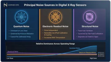
Signal-to-Noise Ratio and Noise Sources
Three principal noise contributors govern SNR in digital X-ray sensors:
Quantum noise arises from photon statistics—the inherent randomness in X-ray photon arrival follows Poisson distribution. This noise dominates at low dose and sets the fundamental detection limit for subtle density variations. Unlike electronic noise, quantum noise cannot be reduced through calibration—only higher dose reduces it.
Electronic readout noise includes fixed pattern noise and dark current from TFT leakage. Unlike quantum noise, electronic noise is dose-independent and can be reduced through offset calibration and cooling. Dark current increases with temperature, making thermal management critical in hot industrial environments.
Structural noise reflects fixed gain variations across the detector array—pixel-to-pixel sensitivity differences that remain after factory calibration. Gain calibration using flat-field correction normalises these variations, but calibration accuracy degrades as detectors age or environmental conditions shift.
Each noise type exhibits distinct dependencies on dose and spatial frequency. Their relative weighting shifts across the sensor's operating range—quantum noise dominates low-dose operation, whilst electronic noise sets the floor for high-dose measurements.
These noise characteristics collectively determine the sensor's practical sensitivity threshold—the minimum signal it can reliably detect above the noise floor.
Sensitivity and Dark Current
Sensitivity defines the minimum detectable signal above the noise floor—the threshold below which measurement uncertainty exceeds the signal of interest. Dark current establishes this baseline by generating background charge even without X-ray exposure.
Because dark current is temperature-dependent, thermal management becomes an operational concern in industrial environments where ambient temperatures near extrusion lines, steel processing equipment, or curing ovens can exceed 40°C. Uncooled detectors experience significant dark current drift across temperature swings, requiring more frequent recalibration to maintain measurement accuracy.
How Digital X-Ray Sensors Are Specified, Validated, and Maintained
Industrial X-ray sensor datasheets specify DQE, MTF (at multiple spatial frequencies), pixel pitch, active area, frame rate, and energy range. These rated values come from controlled test conditions that rarely match actual process geometry or material behavior.
The difference between rated DQE at 1 lp/mm with a standard phantom and field-measured DQE under actual production conditions can exceed 20-30%. Scatter radiation from thick or dense materials, non-uniform beam profiles from aged X-ray sources, and detector calibration drift all degrade real-world performance below datasheet specifications.
Validation and Calibration Methods
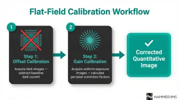
Flat-field correction forms the prerequisite for quantitative industrial use and comprises two steps:
- Offset calibration removes dark current baseline by acquiring images without X-ray exposure, then subtracting this baseline from subsequent measurements
- Gain calibration normalises pixel-to-pixel sensitivity variation by acquiring uniform-exposure images and calculating per-pixel correction factors
Calibration frequency should match detector drift rate and environmental stability — not arbitrary schedules. Per Agfa's detector calibration guidelines, manufacturers typically recommend intervals of 3 to 12 months. In practice, operational triggers matter more: recalibrate after any change in beam energy, material type, or operating temperature, and always after mechanical shock to the detector.
Spatial resolution validation uses bar test patterns or edge response methods, from which MTF is derived. ASTM E2597 employs duplex wire Image Quality Indicators to determine interpolated basic spatial resolution in field conditions. Critically, these measurements must be performed at the energy levels and geometry used in actual production — factory acceptance conditions alone are not sufficient.
Implications of Operating Outside Sensor Specifications
Under-exposure (dose below the sensor's optimal operating range) triggers quantum noise dominance. The image turns grainy, fine structural detail disappears into noise, and density measurements become unreliable. What makes this particularly hazardous is that the degradation builds gradually—out-of-spec operation can persist undetected whilst defects pass through inspection.
That risk of silent failure extends to over-exposure and energy mismatch, which introduce a separate set of problems. Saturated pixels produce bright artefacts in high-density regions, but partial saturation may only compress contrast without obvious visual indicators. Operating at beam energies outside the scintillator's efficient absorption window reduces effective DQE without altering image appearance—the sensor looks functional whilst measurement accuracy is quietly compromised.
Radiation Safety and Regulatory Implications
Industrial X-ray systems require radiation enclosures, interlock systems, and operator dose monitoring under applicable national regulations (including IEC 61267 and EN 62220 in European markets). Implementation costs include:
- Radiation shielding and safety enclosures
- Access interlock systems and emergency shutoff controls
- Personal dosimetry programmes for operators
- Equipment registration with regulatory authorities
- Periodic compliance inspections and documentation
For certain industrial thickness measurement applications—particularly continuous web materials such as nonwovens, films, and textiles—these requirements create significant operational friction. Non-radioactive contactless alternatives such as millimetre-wave (M-Ray) technology can provide comparable or superior measurement accuracy without the radiation safety, licensing, or regulatory compliance overhead. Hammer-IMS, for example, uses M-Ray systems across plastic sheet extrusion, nonwovens, and textile production—providing traceable thickness measurement without ionising radiation.
Common Misinterpretations of Digital X-Ray Sensor Specifications
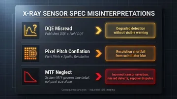
Published DQE and MTF figures represent condition-specific benchmarks, not absolute performance guarantees. Real-world DQE degrades with beam scatter, detector ageing, and miscalibration. The published DQE figure at 0 lp/mm spatial frequency measures detection efficiency only—MTF at higher spatial frequencies governs fine detail discrimination.
Pixel pitch misuse creates systematic over-specification of expected resolution. The smallest resolvable feature depends on complete system MTF (scintillator optical spread, pixel fill factor, and readout electronics bandwidth), not pixel dimensions alone.
A 100 μm pixel pitch does not guarantee 100 μm spatial resolution if scintillator blur or focal spot size degrades system MTF at that frequency.
These misinterpretations have real consequences in practice. In thin-material industrial inspection, buyers often select sensors expecting resolution to match pixel size — then encounter shortfalls driven by overlooked MTF limitations. Common results include:
- Incorrect sensor selection for the application's actual resolution requirements
- Rejected parts or missed defects caused by unverified spatial frequency performance
- Specification disputes between supplier and end-user tracing back to DQE/MTF conflation
Conclusion
Digital X-ray sensors are active measurement systems. Output accuracy depends on sensor design parameters, operating conditions, calibration state, and material-specific penetration physics — and all of these interact. Managing them together, not in isolation, is what delivers reliable measurement in industrial production.
Engineering judgement is required to translate datasheet specifications into appropriate industrial decisions. A sensor optimised for radiology may be the wrong choice for high-speed in-line manufacturing, where dose limits, throughput demands, and regulatory compliance operate simultaneously.
For continuous-web processes in plastics, nonwovens, and textiles, non-nuclear alternatives can deliver equivalent accuracy without the infrastructure burden of X-ray systems. Technologies such as Hammer-IMS's M-Ray millimeter-wave systems, for example, reduce total cost of ownership whilst maintaining — or improving — measurement performance against X-ray baselines.
Frequently Asked Questions
What is the difference between direct conversion and indirect conversion in digital X-ray sensors?
Direct conversion uses a photoconductor (such as amorphous selenium) to convert X-rays directly into electrical charge, offering superior spatial resolution with minimal lateral spread. Indirect conversion uses a scintillator to convert X-rays to visible light before photodetection, which is simpler to manufacture at large scales but loses sharpness due to optical scatter within the scintillator layer.
How does Detective Quantum Efficiency (DQE) affect image quality in industrial X-ray imaging?
Higher DQE means the sensor extracts more usable image information per unit of radiation dose, enabling lower-dose operation without sacrificing image quality. This directly affects the detection threshold for small defects or subtle thickness variations—a sensor with DQE of 0.7 delivers significantly better performance than one with DQE of 0.3 at the same radiation exposure level.
What factors limit the spatial resolution of a digital X-ray sensor?
Spatial resolution is governed by pixel pitch (smaller pixels improve sampling), scintillator optical spread (light scattering in indirect systems), and X-ray source geometry (focal spot size and source-to-detector distance). System MTF mathematically combines all three to determine actual resolution capability.
How often should digital X-ray sensors be recalibrated in industrial settings?
Gain and offset calibration should typically be performed at the start of each shift or after any change in beam energy, material type, or operating temperature. Optimal intervals range from daily to quarterly depending on detector drift rate, temperature stability, and detector age.
What are the regulatory requirements for using digital X-ray systems in industrial manufacturing?
Industrial X-ray systems are subject to national radiation protection regulations requiring radiation enclosures, access interlocks, operator dose monitoring, and equipment registration. Specific requirements vary by country but consistently add cost and procedural complexity to operations.
When is a non-radioactive alternative to X-ray sensing more appropriate for industrial thickness measurement?
Millimetre-wave technologies are well suited to continuous web processes—films, nonwovens, textiles, or foams—where materials are radiation-sensitive or regulatory overhead is prohibitive. They eliminate licensing requirements, reduce operational complexity, and deliver comparable accuracy for appropriate material types and thickness ranges.