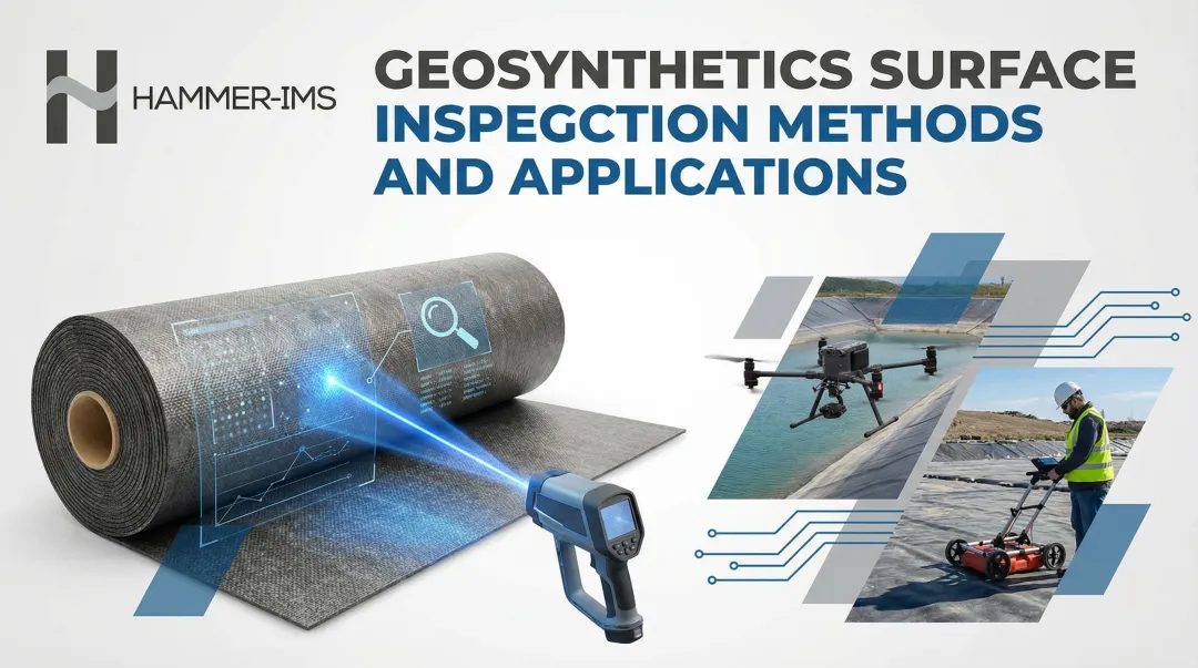
Introduction
Quality managers in high-speed manufacturing face a persistent dilemma: detect microscopic surface defects at full production speeds or risk costly recalls, material waste, and customer complaints. In industries ranging from automotive paint lines to semiconductor wafer fabrication, a single undetected scratch, pit, or contamination particle can cascade into yield losses or field failures. The challenge intensifies when inspection throughput must match line speeds of hundreds of metres per minute whilst detecting anomalies measured in microns.
Laser surface inspection addresses this through non-contact optical techniques that illuminate surfaces with focused light beams and analyse the reflected, scattered, or displaced photons to identify defects, measure profiles, and assess surface quality without touching the material.
This guide covers the core techniques — triangulation, scattering, profilometry, and confocal scanning — their system-level operation, applications across sectors from medical devices to steel production, and the practical limits where laser-only solutions need complementary technologies.
TLDR:
- Laser triangulation and scattering systems deliver up to 392 kHz sampling rates for 100% inline inspection at full production speeds
- Confocal laser scanning achieves nanometre-level surface characterisation for precision optics and semiconductor applications, whilst profilometry quantifies roughness to ISO standards
- Industries from automotive to medical devices deploy laser inspection for defects below human detection thresholds—semiconductor systems detect particles down to 12.5 nm
- Highly reflective, transparent, or textured surfaces pose challenges; web materials needing thickness and basis-weight data require complementary measurement technologies alongside laser inspection
What Is Laser Surface Inspection?
Laser surface inspection is an automated, non-contact quality control method that illuminates a surface with a laser beam and analyses the reflected, scattered, or displaced light. The goal is to identify defects — scratches, cracks, contamination, dimensional deviations — or to quantify surface geometry.
Two standards frame this field: SEMI M59 defines a Scanning Surface Inspection System (SSIS) as an instrument for rapid examination of quality areas to detect localised light scatterers or haze, whilst ISO 25178 classifies non-contact optical methods for measuring 3D areal surface texture.
How it differs from legacy methods:
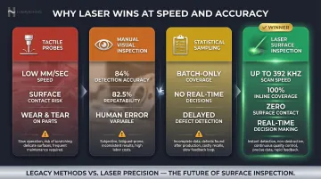
- Versus tactile probes: Laser systems operate at kilohertz sampling rates (up to 392 kHz for the Keyence LK-G5000) compared to millimetre-per-second contact profilometers; no surface contact eliminates wear and contamination
- Versus manual visual inspection: In aerospace blade inspection, 3D laser scanning achieved 100% defect detection and repeatability compared to 84% accuracy and 82.5% consistency for human operators
- Versus statistical sampling: Production-line speeds enable 100% inline inspection rather than batch sampling, with real-time pass/fail decisions within milliseconds
Two Primary Inspection Goals
Laser inspection serves distinct purposes depending on application requirements:
- Defect detection — Identifying anomalies such as pits, burrs, contamination particles, or cracks through analysis of scattered or abnormal reflection patterns
- Surface characterisation — Quantifying roughness (Ra/Rz per ISO 4287), waviness, profile geometry, or 3D topology through height map reconstruction
Which goal takes priority directly determines which optical technique to deploy — a distinction the following sections address for each major method.
Key Laser Surface Inspection Techniques
Laser Triangulation
A laser spot or line projects onto the surface at an oblique angle. A position-sensitive detector (CMOS or CCD camera) measures the lateral shift of the reflected spot to calculate height or displacement, enabling 3D profile mapping. The geometric relationship between laser source, target, and detector forms a triangle—hence the name.
Typical use cases:
- Inline thickness measurement of flat products (steel plate, plastic sheet) with tolerances better than 1 mm/m
- Surface profile scanning to detect height variations like warps, burrs, or raised edges on metals and polymers
- Gap and flush inspection in automotive assembly, verifying door panel flushness within 0.3 mm and gap consistency within 0.2 mm
The Keyence LJ-V7000 delivers 64,000 profiles per second (64 kHz), achieving 12.8 million points per second—240 times faster than conventional devices.
Laser Scattering (Light Scattering Inspection)
A laser beam illuminates the surface while detectors at defined angles capture the scattered light. The intensity and angular distribution of that scatter reveals particles, contamination, pits, or sub-surface defects.
This technique dominates wafer and precision optics inspection. Specular surfaces produce minimal background scatter, so any defect that disrupts the smooth interface creates a detectable signal contrast.
Key parameters influencing detection sensitivity:
- Shorter wavelengths (deep ultraviolet/DUV) push resolution limits — the KLA Surfscan SP7XP achieves 12.5 nm defect sensitivity on polished silicon
- Normal-incidence with off-axis collection captures defect scatter on polished surfaces; oblique incidence suppresses background scatter on rougher materials
- Phase contrast channels (PCC) exploit polarisation differences to detect shallow bumps and thin-film variations
Tuning these three parameters together determines the minimum detectable defect size — a critical factor when specifying systems for semiconductor yield targets or optics acceptance criteria.
Laser Profilometry
Profilometers scan a focused laser spot across the surface to build a high-resolution height map. The z-axis displacement derives from focus or triangulation principles, delivering quantitative roughness values (Ra, Rz per ISO 4287 for 2D profiles; Sa, Sz per ISO 25178-2 for 3D areal parameters) and 3D topology data.
Applications:
- Metrology labs characterising precision machined components, coatings, and microelectronics
- Inline quality gates verifying surface finish compliance to specifications
- Power Spectral Density (PSD) analysis for silicon wafer surface roughness across spatial frequencies, combining optical profiling and atomic force microscopy data
Selecting between 2D and 3D measurement standards depends on whether a single cross-sectional profile suffices or whether areal coverage is needed to capture directional surface textures:
| Standard | Type | Key Parameters | Description |
|---|---|---|---|
| ISO 4287:1997 | 2D Profile | Ra, Rz, Rq | Arithmetic mean deviation, maximum height measured along a single line |
| ISO 25178-2:2012 | 3D Areal | Sa, Sz, Sq | Arithmetic mean height, maximum height measured across a 3D surface area |
Confocal Laser Scanning
Confocal microscopy employs a pinhole aperture in the conjugate image plane to collect only in-focus reflected light, physically rejecting out-of-focus scatter. This optical sectioning enables extremely high axial resolution—sub-micron to nanometre-level—for measuring fine surface textures, thin films, and transparent layer thicknesses.
Performance benchmarks:
- Olympus LEXT OLS4100: 10 nanometre Z-axis resolution
- Keyence VK-X Series: 0.5 nanometre measuring resolution
- Sensofar S neox: 2 nm system noise using a 150X objective in confocal mode
Where confocal inspection is most valuable:
- Precision optics requiring nanometre-level surface characterisation
- Semiconductor wafer surfaces and advanced packaging
- Transparent layer thickness measurement in thin films and coatings
How Laser Surface Inspection Systems Work
Core System Architecture
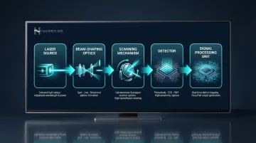
Every laser inspection system integrates five fundamental subsystems:
- Laser source — Wavelength and power selected for material and defect size (visible, infrared, or DUV); typical powers range from milliwatts (Class 1-2) to hundreds of milliwatts (Class 3B-4)
- Beam-shaping optics — Lenses and mirrors focus the beam to the required spot size and shape (point, line, or structured pattern)
- Scanning mechanism — Galvanometer mirrors (up to 1 kHz scan rate), polygon mirrors (exceeding 50,000 RPM for 260 m/s spot speeds), or linear stages (up to 5 m/s for heavy-duty positioning)
- Detector — Photodiode, CCD/CMOS camera, or photomultiplier tube converts optical signal to electrical output
- Signal processing unit — Converts detector output into defect maps, dimensional measurements, or pass/fail decisions
Angle of Incidence and Collection Geometry
Surface type dictates optical configuration:
- Polished or specular surfaces: Normal incidence with off-axis collection captures scattered defect signals while rejecting the strong specular reflection
- Rough or matte surfaces: Oblique incidence with side-collection optics suppresses background surface scatter, improving defect-to-noise ratio
On highly textured metallic surfaces, optical interference within a standard laser point causes speckle-induced measurement errors; laser line sensors compensate by averaging the profile.
Calibration Standards and Traceability
System software compares measured signals against reference baselines or calibration standards. SEMI M53 outlines the practice for calibrating SSIS darkfield channels using certified depositions of monodisperse polystyrene latex (PSL) spheres to assign a Light Scattering Equivalent (LSE) diameter. Thermo Scientific provides NIST-traceable PSL size standards (20 nm to 2,000 µm) for ISO 9000 compliance traceability.
Because real defect morphology is unknown, systems report sizes in LSE diameters based on PSL spheres—but repeated DUV exposure degrades PSL spheres, so silica nanoparticles are often used for calibration and mathematically assigned an equivalent PSL diameter.
Real-Time Data Output and Process Integration
Systems generate defect maps, size distributions, and pass/fail decisions within milliseconds. Data feeds into Statistical Process Control (SPC) and Manufacturing Execution Systems (MES) via standards such as SEMI E30 (GEM) and SEMI E5 (SECS-II), enabling real-time alarms or adjustments to upstream equipment (extrusion die gap, calender pressure, coating thickness).
Industrial Applications Across Sectors
Semiconductor and Electronics Manufacturing
Laser scattering systems scan silicon wafers for sub-micron particle contamination or surface scratches that compromise yield. The KLA Surfscan SC1 inspects up to 110 wafers per hour (200 mm), detecting defects down to 26–34 nm PSL on compound semiconductors (SiC, GaN).
Confocal systems measure thin oxide layer uniformity and advanced packaging bond interfaces. The Onto Innovation Dragonfly G5 extends this to hybrid bonding applications, detecting defects down to 150 nm.
Automotive and Metals
- Painted car bodies: Phase-measuring deflectometry systems detect paint defects with detection rates exceeding 98.5%, identifying sub-millimetre dents or orange peel texture
- Rolled steel: Laser light-section sensors measure flatness of heavy steel plates achieving tolerances better than 1 mm/m and detect surface cracks inline
- Machined parts: Profilometers verify dimensional conformance and surface finish per ISO 4287 roughness specifications
Medical, Aerospace, and Specialty Materials
- Medical devices: ISO 25539-2 specifies requirements for evaluating vascular stents; ISO 25178 3D areal parameters (Sa, Sz) characterise complex implant surfaces and osseointegration zones
- Plastic films and sheet goods: Inline thickness profile monitoring and surface defect detection at production speeds
- Glass inspection: Detection of chips, inclusions, and surface scratches on precision glass substrates
- Aerospace components: Chromatic confocal and terahertz systems provide non-contact, real-time thickness measurements of wet and dry aerospace coatings to optimise fuel efficiency and reduce weight
Across all these sectors, the core challenge is the same: catching defects early enough to act. The technique that works for a 30 nm semiconductor scratch differs fundamentally from what's needed to profile a moving web of nonwoven textile — and choosing the right approach determines whether inspection adds value or just adds cost.
Advantages and Limitations of Laser Surface Inspection
Advantages
Speed and throughput:
| System | Technology | Sampling Rate | Key Advantage |
|---|---|---|---|
| Keyence LJ-V7000 | 2D/3D Laser Profiler | 64 kHz | 12.8 million points/sec—240x faster than conventional devices |
| Keyence LK-G5000 | 1D Laser Displacement | 392 kHz | 392 kHz captures high-frequency vibration events that lower-rate sensors miss |
| LMI Gocator 2500 | 3D Laser Line Profiler | 10 kHz | Onboard processing at 10,000 profiles/sec |
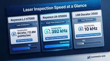
Laser triangulation and scattering enable 100% inline inspection at production speeds, a physical impossibility for tactile coordinate measuring machines (CMMs) or manual sampling.
Additional benefits:
- Preserves delicate surfaces with no probe contact, eliminating wear entirely
- Catches defects invisible to manual inspection — down to 12.5 nm on semiconductor wafers
- Generates quantitative data for statistical process control (SPC) and ISO 9000 traceability
- Delivers repeatable, objective results that remove human variability from the equation
Limitations and Practical Constraints
Not every surface or environment is well-suited to laser inspection. Three material categories create consistent difficulty:
Surface and material challenges:
- Highly specular (mirror-like) surfaces overwhelm detectors with reflected light unless collection geometry is carefully optimised around the reflection angle
- Transparent materials introduce spherical aberration at refractive index boundaries, broadening the point-spread function, reducing peak signal intensity at depth, and distorting Z-axis scaling in confocal systems
- Highly textured or porous surfaces generate high background scatter, masking small defects and degrading signal-to-noise ratio
Operational constraints:
- Laser safety: Class 3B and Class 4 internal lasers achieve Class 1 system ratings through protective housings and safety interlocks per IEC 60825-1:2014 — but those enclosures and interlocks add cost and integration complexity
- Laser-based thickness measurement depends on surface reflection, making it less reliable for composites, multilayer materials, or products where internal structure, not surface geometry, determines product quality
When Laser Inspection Alone May Not Be Enough
For continuous web materials—nonwovens, technical textiles, plastic films, foam—surface inspection is only part of the quality picture. Thickness uniformity and basis weight across the full web width are equally critical quality parameters, yet laser surface scanners alone do not capture these cross-sectional properties. A laser triangulation system detects surface height variations but cannot distinguish whether a thickness change results from surface topology or internal density variation.
To close these gaps, manufacturers pair laser surface inspection with non-contact, non-nuclear measurement technologies. Hammer-IMS's M-Ray technology, for example, delivers contactless thickness and basis weight measurement across web materials using electromagnetic millimeter waves rather than optical reflection. Unlike laser systems constrained by line-of-sight and material reflectivity, M-Ray operates through the material itself—measuring products up to 30 cm thick and resolving basis-weight variation down to 1 gsm.
The system provides real-time closed-loop feedback to production equipment, communicating via industrial protocols including Modbus TCP/IP and OPC/UA to adjust die gaps, calender pressure, or extrusion speed as conditions change.
Together, the two technologies address distinct but complementary failure modes:
- Laser surface inspection — detects scratches, contamination, surface roughness, and topographic defects
- M-Ray cross-sectional measurement — verifies thickness uniformity and density distribution through the full material depth
Deployments across foam, plastic sheet, and nonwovens production show that combining both systems reduces waste and enables tighter process control than either approach can achieve independently.
Frequently Asked Questions
What is laser inspection?
Laser inspection is a non-contact measurement technique that uses focused laser beams to detect surface defects, measure geometry, or assess material properties. The system analyses how laser light reflects, scatters, or displaces when it interacts with the target surface, enabling automated quality control at production speeds.
How does a laser profilometer work?
A laser profilometer projects a focused laser spot onto the surface and measures the height of each scanned point using triangulation or autofocus principles. The result is a high-resolution 3D height map quantifying roughness, waviness, and surface texture for metrology and quality assurance.
What types of defects can laser surface inspection detect?
Laser systems detect scratches, pits, cracks, contamination particles, burrs, dimensional deviations, surface roughness variations, and coating non-uniformities. Detection sensitivity depends on the specific laser technique and system configuration—scattering-based systems detect particles down to 12.5 nm on semiconductor wafers, whilst triangulation systems identify sub-millimetre height variations on automotive panels.
What industries use laser surface inspection systems?
Key sectors include:
- Semiconductor — wafer defect detection
- Automotive — paint and panel inspection
- Aerospace — coating thickness and fatigue crack detection
- Medical devices — implant surface characterisation
- Metals and steel — flatness and surface crack assessment
- Plastics and film — thickness profile and defect detection
- Glass manufacturing — chips and inclusion detection
What is the difference between laser triangulation and laser scattering for surface inspection?
Triangulation measures surface height and profile by detecting the geometric displacement of reflected light, enabling 3D mapping and dimensional measurement. Laser scattering detects tiny particles or defects by measuring the intensity of light scattered off the surface at angles away from the specular reflection, revealing contamination or anomalies invisible to triangulation-based systems.
What are the limitations of laser surface inspection?
Highly reflective or transparent surfaces and high surface texture can reduce effectiveness — transparent materials cause spherical aberration in confocal systems, whilst textured surfaces generate background scatter that masks small defects. Materials where internal properties determine quality may also fall outside laser inspection's scope. Complementary non-contact methods, such as electromagnetic or ultrasonic technologies, are often required alongside laser inspection in these cases.