Introduction
Conformal coating thickness sits at the center of PCB reliability. Too thin, and electronics remain exposed to moisture, dust, and corrosion. Too thick, and thermal stress cracks solder joints and damages components. A study on polyurethane coatings found that 130 µm thickness caused 100% of BGA solder joints to fail after 3,500 thermal cycles, illustrating the mechanical risks of overcoating. In contrast, inadequate coating leaves PCBs vulnerable to electrochemical migration and dendritic growth, leading to electrical shorts.
Getting thickness right starts with selecting the correct measurement method for your substrate, production speed, and accuracy requirements. This guide covers wet film, dry film, contact, and non-contact methods: when to use each and how to build a process that delivers consistent quality.
Key Takeaways
- Coating thickness is tightly specified by type: too thin means inadequate protection, too thick means mechanical stress and component failure
- Two measurement categories exist: wet film (during application) and dry film (after curing), with both contact and non-contact options
- Non-contact inline systems enable 100% inspection without slowing production or damaging sensitive assemblies
- Method selection depends on substrate type, inspection area access, required precision, and production throughput
- Process repeatability — calibration, test coupons, data logging, and closed-loop feedback — matters as much as the measurement tool
What Is Conformal Coating Thickness and Why Does It Matter?
Conformal coating is a thin, protective polymeric film applied to PCBs and electronic assemblies to guard against moisture, dust, chemicals, and temperature extremes. Common types include acrylic (AR), epoxy (ER), polyurethane (UR), silicone (SR), and parylene (XY). Getting the thickness right is where coating protection succeeds or fails — too thin and the board is exposed, too thick and the coating itself becomes a liability.
The Dual Failure Risk
Undercoating consequences:
- Leaves PCB vulnerable to environmental damage
- Reduces dielectric protection
- Enables electrochemical migration (ECM) between conductors
- Leads to dendritic growth and electrical shorts under voltage
Overcoating consequences:
- Creates excessive mechanical stress on components during thermal cycling
- Causes solder joint cracking, particularly on BGA packages
- Risks delamination from substrate
- Induces component failure through repetitive stress
These failure modes become far more consequential in high-stakes applications — where a field failure means more than a warranty claim.
Where Precision Matters Most
Thickness tolerances carry real consequences across four industries in particular:
- Automotive electronics – vibration, heat, and humidity demand full coverage, but overcoating creates mechanical stress that cracks solder joints under engine-bay thermal cycling
- Aerospace assemblies – altitude-driven temperature swings of 150°C+ require tightly controlled coating thickness to avoid delamination
- Medical devices – regulatory standards (IEC 60601, ISO 13485) require documented coating uniformity as part of device safety validation
- Industrial automation – corrosion resistance is critical, but overcoating risks thermal stress failures in sealed enclosures
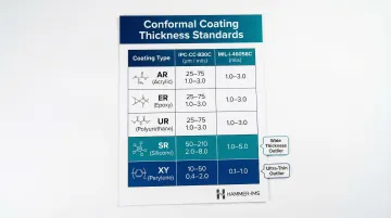
Recommended Conformal Coating Thickness Standards
The industry relies on two primary standards: IPC-CC-830 (the current commercial benchmark) and MIL-I-46058C (inactive for new designs since November 1998 but still required for legacy defence contracts).
Standard Thickness Ranges by Coating Type
| Coating Type | Chemistry | IPC-CC-830C Range (µm) | IPC-CC-830C Range (mils) | MIL-I-46058C Range (mils) |
|---|---|---|---|---|
| AR | Acrylic Resin | 25–75 µm | 1.0–3.0 mils | 1.2–5.0 mils |
| ER | Epoxy Resin | 25–75 µm | 1.0–3.0 mils | 1.2–5.0 mils |
| UR | Polyurethane Resin | 25–75 µm | 1.0–3.0 mils | 1.2–5.0 mils |
| SR | Silicone Resin | 50–200 µm | 2.0–8.0 mils | 2.0–8.0 mils |
| XY | Parylene | 12.5–75 µm | 0.5–3.0 mils | 0.4–2.0 mils |
Job-Specific Specifications
These standards define acceptable ranges — the actual specified thickness is set at the assembly level. In practice:
- The quality specification for each project determines the target thickness
- Measurement results always compare against the job-specific requirement, not a generic standard range
- Generic ranges serve as guardrails, not pass/fail criteria on their own
The 80/20 Rule for Coatings
The 80/20 rule requires that coating cover at least 80% of specified areas to the required depth. The remaining 20% tolerance accommodates complex features — component leads, tall components, and tight geometries — where physically uniform coverage is difficult.
This directly shapes measurement sampling strategy. Measurement points should target both flat areas, where minimum thickness must be confirmed, and complex geometries, where the 20% tolerance comes into play.
Methods for Measuring Conformal Coating Thickness
Measurement methods fall into two timeline stages (wet vs. dry film) and two contact categories (contact vs. non-contact). The best choice depends on substrate type, required precision, and whether inline or offline measurement is acceptable.
Wet Film Measurement
Wet-film comb gauges work by pressing graduated teeth into the wet coating immediately after application. The last wetted tooth indicates current thickness. This reading must then be converted to expected dry film thickness using the coating's solids content:
Dry Film Thickness = Wet Film Thickness × % Solids by Volume
Comb gauges are inexpensive and fast — useful for catching process drift before curing. But they sample only a single point, leaving uniformity across the PCB unconfirmed. Per ASTM D4414, they are "neither accurate nor sensitive" enough for final quality assurance. Use them for in-process control, not final validation.
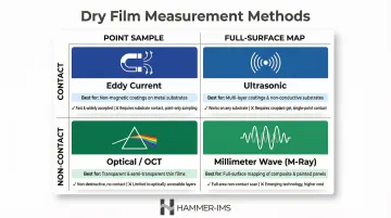
Dry Film Measurement — Contact Methods
Eddy Current Gauges
Eddy current gauges (e.g., DeFelsko PosiTector 6000) measure the distance from probe to the copper ground plane beneath the coating.
High-precision models achieve accuracy to ±1 µm, but two conditions must be met: a continuous copper ground plane must exist in the measurement area, and the gauge must be zeroed on the solder mask — not bare copper. Zeroing on bare copper causes the gauge to include solder mask thickness in the reading, producing systematically inflated results.
Caliper/Micrometer Subtraction Method
Measure PCB thickness before coating and after curing. The difference, averaged across multiple points, yields coating thickness.
Divide by two when both sides are coated. Standard deviation analysis across measurement points gives a rough uniformity picture. The method is susceptible to errors from coating topography and substrate compressibility, making it a fallback option when dedicated gauges aren't available.
Ultrasonic Measurement
Ultrasonic gauges emit a pulse and measure the echo return time from the substrate interface. For PCB applications, this approach has significant constraints: it requires a couplant (water or glycol gel), the layered FR-4 structure produces confusing acoustic signals, and zeroing on multilayer boards is unreliable. It works best on thick silicone coatings or simple 2-layer boards where the acoustic path is cleaner.
Dry Film Measurement — Non-Contact and Inline Methods
Optical and Spectral Methods
Non-contact optical methods — including hyperspectral/NIR imaging and Optical Coherence Tomography — analyze how light interacts with the coating across the full PCB surface simultaneously.
These methods produce 2D thickness maps rather than point samples, enabling 100% inline inspection without physical contact. OCT achieves axial resolution of 1.72 µm, making it one of the most precise non-destructive options available for production line monitoring.
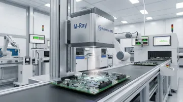
Hammer-IMS M-Ray Technology
Hammer-IMS's M-Ray millimeter wave technology operates at 60 GHz electromagnetic frequency to deliver contactless thickness measurement in inline production environments.
Key capabilities:
- Contactless measurement — no couplant, no physical probe contact
- Real-time output suitable for continuous 100% inline inspection
- High standoff distance keeps the sensor clear of hot or sensitive board surfaces
- No radioactive sources, meeting workplace safety requirements for electronics environments
This makes M-Ray well-suited for production environments moving from offline batch sampling to continuous inline inspection.
Destructive Methods
Cross-Sectioning (Microsectioning per IPC-TM-650)
Cut a sample, mount it in plastic, polish it, and examine it under a microscope to measure coating height.
Cross-sectioning provides the most accurate measurement available and serves as the reference method for calibrating other techniques. Because it destroys the board, it's limited to batch sampling and root cause investigation — not routine production QC.
How to Build a Reliable Conformal Coating Measurement Process
Selecting the right gauge is only the starting point. A reliable measurement process connects specification definition, tool selection, calibration, and closed-loop feedback into a single workflow — so every result is actionable.
Step 1 — Define Your Thickness Specification
Before any measurement begins:
- Identify the coating type (AR, ER, UR, SR, XY)
- Map it to the relevant IPC or customer-specific thickness range
- Document the job-specific minimum and maximum acceptable dry film thickness
- Specify measurement point locations and sampling frequency
Documented acceptance criteria prevent disputes when borderline results appear and give operators a clear reference at every stage.
Step 2 — Select and Set Up the Right Measurement Tool
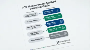
Match the tool to your substrate and production requirements:
| Substrate Condition | Recommended Method |
|---|---|
| Boards with accessible copper ground plane | Eddy current gauge |
| Boards without copper ground plane | Ultrasonic gauge or non-contact optical |
| Heavily populated boards with no flat measurement area | Substitution coupons (coat a metal coupon alongside PCB) |
| High-volume production requiring 100% inspection | Inline non-contact systems (optical or millimeter wave) |
| Batch sampling or validation | Eddy current or cross-sectioning |
For densely populated assemblies with no accessible flat area, coat an aluminium or steel coupon alongside the production boards. Measuring the coupon with a standard eddy current gauge gives a reliable surrogate reading for the actual PCB coating thickness.
Step 3 — Calibrate and Verify Before Each Run
All contact gauges must be properly calibrated to eliminate systematic error:
1-Point Adjustment (Zeroing):
- Zero eddy current gauges on the solder mask, not bare substrate
- This removes bias from the solder mask layer
2-Point Adjustment:
- Use certified calibration standards at zero and a known thickness slightly above your target
- Fixes the calibration curve across your specific measurement range
- Required per ASTM D7091 for coating thickness measurement
Verification frequency:
- Verify gauge accuracy on reference standards before critical measurements
- Re-verify at the start of each shift
- Document verification results for traceability
Step 4 — Measure, Sample, and Record
Define a sampling plan:
- Offline inspection: Specify minimum measurement points per board (typically 5–10) and their exact locations
- Target flat unpopulated areas over ground planes for contact methods
- Measure near complex features separately to verify 80/20 rule compliance
- Inline systems: Configure continuous data capture with timestamp and batch code logging
Recording requirements:
- Log measurements with timestamps
- Link data to batch codes or serial numbers
- Enable traceability and trend analysis
- Support statistical process control (SPC) charting
Step 5 — Compare Results, Feed Back, and Adjust
Compare measured thickness values against the specification in real time. Any out-of-spec result triggers investigation and process adjustment before the next batch.
Closed-loop feedback parameters:
- Spray pressure adjustment (for selective coating)
- Dip speed or withdrawal rate (for dip coating)
- Coating concentration or viscosity
- Conveyor speed or cure temperature
Hammer-IMS's Connectivity 3.0 software supports automated closed-loop control, adjusting process parameters in response to live measurement data. This reduces scrap and rework whilst maintaining tighter thickness tolerances across batches.
How Hammer-IMS Can Help With Conformal Coating Thickness Measurement
Hammer-IMS uses M-Ray millimeter wave technology to measure coating thickness without physical contact — directly on the production line, at full throughput. Unlike nuclear-based gauges, M-Ray requires no radioactive sources and no radiation licensing, which simplifies compliance for electronics manufacturers operating under EU or international safety frameworks.
Key Advantages for Conformal Coating Applications
Non-nuclear, operator-safe technology:
- No radioactive sources — no licensing, no radiation safety programs
- Safe for operators working near sensitive electronic assemblies
- Eliminates the compliance overhead tied to nuclear measurement equipment
Inline, non-contact measurement:
- High standoff distance keeps the sensor clear of components and coatings
- Real-time data capture at production speed, no throughput penalty
- Connectivity 3.0 software feeds thickness data back to the line for closed-loop correction
Moving from batch sampling to 100% inspection:
For manufacturers currently pulling boards for offline spot-checks, inline M-Ray measurement is a direct upgrade. Deviations get caught mid-run — not after an entire batch has been coated.
- Reduces material waste by catching deviations before full-batch commits
- Improves first-pass yield through real-time process feedback
- Supports traceability and compliance with IPC coating standards
- Recipe configuration and data logging provide audit-ready production records
Conclusion
Conformal coating thickness sits in a narrow acceptable window. Missing that window in either direction carries real consequences: inadequate protection leads to electrochemical migration and field failures, whilst excessive thickness causes mechanical stress and solder joint cracking.
Achieving consistent results comes down to three connected steps:
- Select the right measurement method for your substrate type and production environment
- Build a documented process with defined specifications, calibration schedules, strategic sampling, and data logging
- Implement closed-loop feedback to adjust coating application in real time rather than catching defects after the fact
That last step is where reactive quality control ends and genuine process control begins. Manufacturers who close that loop consistently hit IPC thickness targets, reduce rework, and keep scrap rates low.
Frequently Asked Questions
How to measure the thickness of conformal coating?
The right method depends on whether the coating is wet or cured and whether the board has a copper ground plane. Wet film comb gauges monitor coating volume during application; for cured coatings, eddy current probes suit boards with ground planes, ultrasonic gauges work without them, and non-contact millimeter wave systems enable inline measurement.
What is the thickness of conformal coating?
Per IPC-CC-830 standards, acrylic, epoxy, and polyurethane coatings typically range from 25–75 µm (1.0–3.0 mils), silicone from 50–200 µm (2.0–8.0 mils), and parylene from 12.5–75 µm (0.5–3.0 mils). The exact required thickness is always defined at the job level in the assembly's quality specification, not just by the generic standard range.
What is the 80/20 rule for coating?
The 80/20 rule states that at least 80% of a coated assembly must achieve the minimum specified thickness, while up to 20% tolerance is allowed for areas around tall components, leads, or complex geometries where uniform coverage is physically difficult to achieve. This guides both measurement placement and interpretation of borderline results.
What is the difference between wet film and dry film conformal coating measurement?
Wet film measurement uses a comb gauge right after application to confirm coating volume before curing, allowing real-time process adjustment. Dry film measurement is taken post-cure using contact or non-contact gauges to verify final thickness against the quality specification.
Can conformal coating thickness be measured without destroying the PCB?
Yes. Non-destructive methods include eddy current probes (for boards with ground planes), ultrasonic gauges (for boards without ground planes), hyperspectral imaging, Optical Coherence Tomography (OCT), and millimeter wave contactless systems like Hammer-IMS's M-Ray technology. All these methods measure coating thickness without cutting or damaging the board, making them suitable for inline or 100% inspection programmes.