Introduction
Silicon anodes expand by up to 300% during lithiation — a volumetric shift that graphite electrodes never experience. That expansion transforms coating thickness from a simple dimensional spec into a parameter that directly governs capacity output, cycle life, and structural integrity.
Many battery manufacturers find themselves caught between areal capacity targets and the mechanical stresses silicon expansion creates. Hitting both requires precise thickness specification and real-time process control. Unlike graphite systems, where coating tolerances are more forgiving, silicon anodes demand tight control at two distinct levels: electrode-level coatings and nano-scale surface treatments — each serving separate functions with separate failure modes.
Key Takeaways
- Electrode coatings for silicon anodes typically target 50–150 µm dry thickness, driven by areal capacity targets and silicon content
- Silicon's 300% expansion during lithiation forces designers to set initial thickness with post-cycling dimensional change in mind
- Surface passivation coatings (2–100 nm) stabilise the SEI layer and demand tighter tolerances than bulk electrode coatings
- Thickness deviations hurt performance: too thick raises ionic resistance and delamination risk; too thin cuts usable capacity
- Inline, non-contact gauging keeps thickness uniform along the electrode web — catching drift before it becomes scrap
What Anode Coating Thickness Means in Silicon Batteries
Electrode-Level vs. Particle-Level Coatings
Anode coating thickness at the electrode level refers to the dried, calendered active material layer deposited on a copper current collector during slurry casting. This layer contains silicon particles, binder, and conductive additives, and is measured in micrometers (µm). It is distinct from the nano-scale surface coatings applied to individual silicon particles.
Electrode coating thickness is a design parameter, not merely a process outcome. Engineers deliberately specify this dimension to:
- Hit areal capacity targets (mAh/cm²)
- Constrain stack height within cell packaging limits
- Ensure electrolyte access through controlled porosity
- Balance energy density against mechanical resilience
The Silicon-Specific Challenge
Unlike graphite electrodes, silicon coatings must accommodate volumetric expansion exceeding 300% during cycling. Specifying a target dry thickness is only the starting point; the electrode must retain structural cohesion through repeated dimensional change across thousands of cycles.
The theoretical capacity for Li₁₅Si₄ at room temperature reaches 3,579 mAh/g. Reaching that figure in practice means managing the physical consequences of lithium-silicon alloying at every stage of the coating's life.
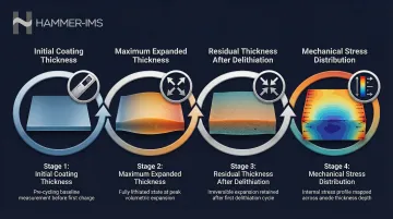
This expansion constraint means silicon anode thickness specifications must account for:
- Initial coating thickness (pre-cycling)
- Maximum expanded thickness (fully lithiated state)
- Residual thickness after delithiation (irreversible expansion)
- Mechanical stress distribution through the coating depth
Recommended Coating Thickness Ranges for Silicon Anodes
No single universal standard applies across all silicon battery formats. Thickness ranges are governed by cell chemistry, active material content, and areal capacity targets.
Electrode-Level Coating Thickness
Typical dry coating thickness for silicon-dominant anodes: 38–53 µm for single-sided coatings targeting 2.0–3.7 mAh/cm² areal capacity. Exact values depend directly on silicon content:
- Silicon-graphite composites (15 wt% Si): 53 µm dry thickness, 42.6% porosity, 6.21 mg/cm² loading achieves 3.7 mAh/cm²
- Higher silicon content electrodes: Thinner coatings required to manage expansion stress
- Pure silicon anodes: Typically stay at the lower end of the range (38–50 µm)
The broader industry range extends to 50–150 µm when accounting for varying silicon percentages and cell designs, though most production cells cluster in the 40–60 µm zone.
Wet-to-Dry Coating Dynamics
The wet coating thickness applied by slot-die or doctor blade exceeds the final dry value due to solvent evaporation. This wet-to-dry ratio is a critical process parameter tied to slurry solid content:
| Wet-Gap Height | Drying Shrinkage | Implication |
|---|---|---|
| 100 µm | 60% | High solvent retention leads to greater dimensional change during drying |
| 20 µm | 31% | Lower initial solvent volume reduces shrinkage and improves dimensional control |
For a 40 µm dry target, a slurry at 55% solids content typically requires a gap setting in the 70–75 µm range — a value that must be re-validated whenever slurry formulation changes.
Calendering Impact on Final Thickness
After drying, electrodes are calendered (compressed) to increase electrode density and improve interparticle contact. Calendering reduces thickness further and alters final porosity:
- Uncalendered silicon/graphite electrodes: 60–72% porosity
- Typical calendering compression: ~30% thickness reduction
- Target post-calendering porosity: 30–42%
Calendering to 30% porosity triggers severe lithium metal plating, while leaving electrodes at 40% porosity accelerates Li⁺ loss to the SEI, reducing cycle life from 347 down to 225 cycles. This narrow 30–40% porosity window creates a critical design constraint that directly impacts allowable coating thickness.
Nano-Scale Surface Coating Thickness
A secondary coating category operates at the particle level: conductive polymer or inorganic coatings (e.g., PEDOT, carbon, Al₂O₃) applied to stabilize the SEI. These coatings operate in the 2–100 nm range—three orders of magnitude thinner than electrode coatings.
Published research consistently shows thinner coatings (2–15 nm) outperform thicker ones:
| Coating Material | Optimal Thickness | Performance Outcome |
|---|---|---|
| PEDOT (polymer) | 2–15 nm | ~7% capacity retention improvement, ~18% cycle life increase vs. uncoated Si |
| Carbon (RF resin) | 10 nm | 1,006 mAh/g capacity with >99.5% Coulombic efficiency after 500 cycles |
| Al₂O₃ (ALD) | 2–5 nm | Thinner SEI formation, 95% capacity retention with 4 nm coating |
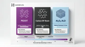
Excessive thickness above 80–100 nm blocks pores and raises resistance, suppressing capacity below even uncoated baselines.
Critical distinction: These two thickness categories (µm-scale electrode coating and nm-scale surface coating) serve different functions and require different measurement approaches. Conflating them is a common specification error.
Factors That Define Silicon Anode Coating Thickness Requirements
Volume Expansion and Mechanical Constraints
Silicon expands up to 300% volumetrically during lithiation, causing the electrode coating to physically thicken and then contract on delithiation. Thicker electrode coatings are more prone to:
- Particle cracking and pulverization
- Delamination from the copper current collector
- Loss of electrical contact between active particles
- Continuous SEI rupture and reformation
Silicon content directly correlates with degradation risk:
| Silicon Content (wt%) | Post-Cycling Thickness Increase | Degradation Impact |
|---|---|---|
| 0 (pure graphite) | 4.0% | Minimal swelling |
| 5 | 27.0% | Moderate swelling |
| 10 | 48.2% | Increased electrical isolation risk |
| 15 | 87.2% | Severe swelling, continuous SEI growth |
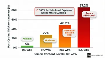
This linear relationship between silicon content and macroscopic electrode swelling forces designers to reduce coating thickness as silicon percentage increases — and makes binder selection a critical decision at higher silicon loadings.
Binder Selection Impact
The choice of binder significantly affects the maximum practical electrode thickness:
- PVDF (polyvinylidene fluoride): Exhibits poor cohesion with silicon, leading to cracks, delamination, and structural collapse during lithiation
- Li-PAA (lithiated polyacrylic acid): Forms strong ion-dipole interactions with silicon particles, demonstrating 81% reversibility of total expansion and enabling practical electrodes with >3 mAh/cm² capacity loading
Li-PAA's superior mechanical resilience allows thicker coatings than PVDF at the same silicon content — in practice, this means achieving capacity loadings above 3 mAh/cm² that would be structurally unstable with PVDF binders.
Areal Capacity and Cell Design Targets
Coating thickness, active material loading (mg/cm²), and areal capacity (mAh/cm²) follow a direct mathematical relationship:
Q_A = ρ Q_S ε_AM L
Where:
- Q_A = areal capacity (mAh/cm²)
- ρ = density (g/cm³)
- Q_S = specific capacity (mAh/g)
- ε_AM = volume fraction of active material
- L = electrode thickness (cm)
The total mass loading relates to thickness and porosity by:
m = (1 - ε) L (ω_AM ρ_AM + ω_C ρ_C + ω_B ρ_B)
Where ω represents weight fractions of active material, conductive agent, and binder.
Higher capacity targets require thicker coatings, but this amplifies all expansion-related risks. Each step up in areal capacity loading compounds the mechanical stress and SEI instability described above.
In prismatic and pouch cells, stack height constraints set a hard ceiling on total electrode thickness. Coating thickness must therefore be optimized within a fixed dimensional envelope — balancing capacity targets against long-term structural stability.
Electrode Porosity and Electrolyte Access
Coating thickness interacts directly with porosity. Thicker coatings create longer Li-ion diffusion paths, making electrolyte infiltration and ionic transport more dependent on pore structure. Target porosity for silicon anode electrodes typically ranges from 30–42% post-calendering, balancing:
- Lower porosity (<30%): Higher volumetric capacity but increased lithium plating risk and reduced rate capability
- Higher porosity (>42%): Better electrolyte access and rate capability but accelerated SEI growth and Li⁺ inventory loss
Staying within this porosity window becomes especially critical at high charge rates. At elevated C-rates, thick electrodes exhibit severe concentration polarization, leading to non-uniform Li intercalation and localized stress concentrations that accelerate degradation.
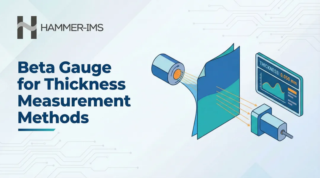
How Anode Coating Thickness Is Measured and Controlled in Production
In silicon anode production, thickness variation across the web—both in machine direction and cross-web—directly translates into cell-to-cell performance inconsistency. Controlling that variation requires understanding where each measurement method works, and where it falls short.
Offline and Spot Measurement Methods
Common offline techniques each cover a distinct measurement need:
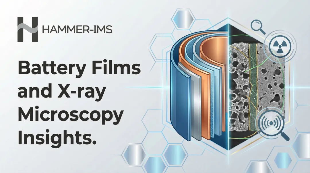
- Cross-Sectional SEM — High-resolution imaging of morphology, porosity, and coating uniformity. Ion milling (FIB or CP) is required to avoid fracture artifacts. Destructive and too slow for production monitoring.
- GD-OES (Glow Discharge Optical Emission Spectroscopy) — Ultra-fast elemental depth profiling from a few monolayers up to ~150 µm; effective for tracking Li inventory and SEI growth. Creates a sputter crater upon use.
- XPS (X-ray Photoelectron Spectroscopy) — Probes only the top 1–10 nm. Suited to ultra-thin nano-coatings and SEI composition analysis, not macroscopic electrode thickness.
- Contact Micrometry/Profilometry — Stylus-based measurement prone to penetrating or scratching porous films; substrate roughness introduces noise. Less reliable for silicon-dominant electrodes.
Every method above is destructive and slow. None can detect within-batch thickness drift while production is running—which is where inline metrology becomes necessary.
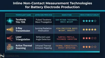
Inline Non-Contact Measurement
Inline systems monitor coating thickness continuously, enabling real-time correction before out-of-spec material advances down the line. The leading technologies are:
| Technology | Operating Principle | Resolution | Production Suitability |
|---|---|---|---|
| Terahertz (THz-TDS) | Time-of-flight detection | 10–300 µm range; <1 µm reproducibility | Excellent; measures wet and dry processes separately |
| X-Ray Transmission | Direct photon beam through electrode | 1–3 mm defect resolution | Superior to beta gauges; no radioactive scatter |
| Laser Triangulation | Angular reflection of laser line | 1 µm accuracy; 0.2 µm repeatability | Good for opaque materials with smooth surfaces |
| Active Thermal Scanning | IR camera monitors temperature decay | ±0.3 mg/cm² mass loading | Simultaneously detects defects and estimates porosity |
Hammer-IMS M-Ray Technology uses electromagnetic millimeter waves (30–300 GHz) for non-contact, non-nuclear measurement. Key capabilities include:
- Eliminates sensor and material wear through fully contactless operation
- Achieves accurate distance measurement via high-frequency time-delay detection
- Works regardless of material color, transparency, or opacity
- Measures hot materials directly after processing, without cooling delays
M-Ray systems integrate with Hammer-IMS Connectivity 3.0 software for real-time feedback and closed-loop process adjustment—correcting slot-die gap, line speed, or slurry flow before out-of-spec material is produced.
Measurement Accuracy and Resolution Requirements
For silicon anode coatings, measurement resolution must detect variations that affect cell performance. Battery electrode lines typically demand sub-micron precision for electrode-level coatings to ensure:
- Areal capacity uniformity within ±0.3 mg/cm²
- Thickness consistency within ±1–2 µm
- Detection of 15–25 µm thickness variations that cause interface degradation
The porous, rough surface of silicon-dominant coatings creates challenges for optical and contact methods. X-ray transmission and millimeter-wave systems average across surface texture rather than reading it as variation—making them the practical choice for production environments where surface roughness would otherwise undermine measurement accuracy.
Consequences of Deviating from Recommended Coating Thickness
Coating thickness deviations affect electrochemical performance, mechanical integrity, and safety — often all three at once.
Too Thick: Performance and Structural Degradation
Above the upper thickness guideline, silicon anodes suffer:
- Longer Li-ion diffusion paths create concentration polarization at high C-rates, raising ohmic and ionic migration resistance despite the larger surface area
- More electrode volume means more initial SEI formation, consuming lithium inventory irreversibly and reducing first-cycle Coulombic efficiency
- Expansion stresses during early cycles can exceed binder tolerance — thickness variations of 15–25 µm between neighboring silicon domains drive severe delamination
- For nano-scale surface coatings, exceeding ~80–100 nm (e.g., PEDOT) blocks pores and impedes Li-ion diffusion, dropping first-cycle Coulombic efficiency to 77.1% versus 80.0% for pristine anodes
Too Thin: Capacity and Stability Shortfalls
Underthick electrodes deliver insufficient areal capacity, compromising cell energy density. For protective surface coatings, insufficient thickness means:
- The SEI remains unstable across cycling
- Continuous electrolyte consumption
- Lithium inventory loss
- Accelerated capacity fade
Incomplete nano-coating coverage leaves silicon directly exposed to electrolyte — even small gaps are enough to restart the degradation cycle.
Uniformity Failures
Thickness and capacity failures aren't limited to under- or over-coating. Even when average thickness is within spec, cross-web non-uniformity creates local variations that:
- Degrade full-cell balance
- Accelerate localized degradation
- Create reproducibility problems across battery packs
- Cause premature cell failure in series-connected modules
Acceptable thickness variation tolerances for battery electrode production are typically ±1–2 µm or ±2–3% of nominal thickness, though specific manufacturers may set tighter internal specifications.
Frequently Asked Questions
What are anode coating thickness standards?
No single universal standard governs silicon anode coating thickness. Values are set by cell designers based on areal capacity targets and silicon content, with typical dry electrode thicknesses ranging from 50–150 µm. Standards such as IEC 61960 define overall cell performance testing but do not mandate specific coating tolerances, which remain proprietary manufacturer specifications.
How do you calculate anode coating thickness?
Electrode coating thickness is derived from target mass loading (mg/cm²) divided by electrode density (g/cm³), accounting for porosity: L = m / [(1-ε)(ω_AM ρ_AM + ω_C ρ_C + ω_B ρ_B)], where L is thickness, m is mass loading, ε is porosity, and ω/ρ are the weight fractions and densities of active material, conductive agent, and binder. Wet thickness also accounts for solvent volume lost during drying.
How thick is anode copper foil?
Copper current collector foil for lithium-ion battery anodes typically ranges from 6 to 15 µm in thickness, with modern high-energy cells targeting 6–10 µm to maximize gravimetric energy density. This dimension is distinct from the active material coating deposited on top of the foil.
What happens if the silicon anode coating is too thick?
Excessive electrode coating thickness increases ionic diffusion resistance, raises the risk of mechanical cracking due to silicon expansion, and can reduce first-cycle efficiency. For nano-scale surface coatings, thicknesses above ~80–100 nm block pores and suppress capacity below even uncoated baselines.
How does silicon's volume expansion affect coating thickness guidelines?
Silicon expands up to 300% during lithiation, meaning the electrode physically changes thickness during each charge cycle. This forces designers to set tighter initial thickness tolerances and use flexible binders. Any pre-existing non-uniformity is amplified by repeated expansion and contraction, accelerating delamination and electrical isolation.